
I. INTRODUCTION
This study presents a unified approach for predicting the reflectance and transmittance properties of multilayer optical thin films and multilayer quantum well-and-barrier structures using the same unified set of equations. Replacing certain classical electrodynamic quantities in these equations with certain relativistic quantum-mechanical quantities is required in this unified approach. See Table (1). The underlying key equations necessary for deriving these unified sets of equations are the Maxwell vector field [1] and newly developed relativistic Dirac vector field equations [2] and [3].
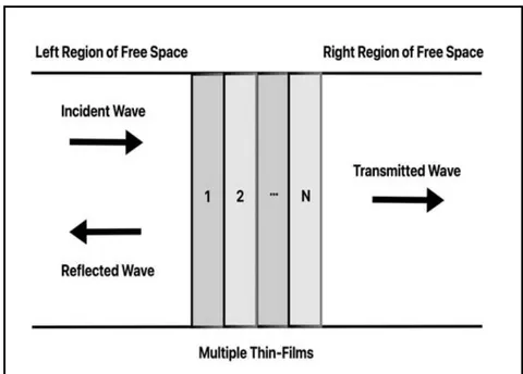
Figure 1 depicts an incident wave impinging on a multilayer thin-film structure at normal incidence. This gives rise to both a reflected wave and a transmitted wave. For the optical thin-film case, a photon and its associated electromagnetic wave serve the purpose. For the quantum thin-film case, an electron and its associated matter wave are the particle and wave of interest. and represent the probabilities a particle will be either reflected or transmitted. Assuming no absorption takes place within the thin film, then .
The emphasis of this study was on the analysis of a single thin film with parallel planar boundaries. The results for this case can then be easily generalized to handle multilayer thin-film structures consisting of thin films. For a single optical thin film, the permittivity , permeability and thickness are important properties of interest. For a single quantum thin film, the thickness and potential energy of electrons moving within the thin film are important quantities of interest.
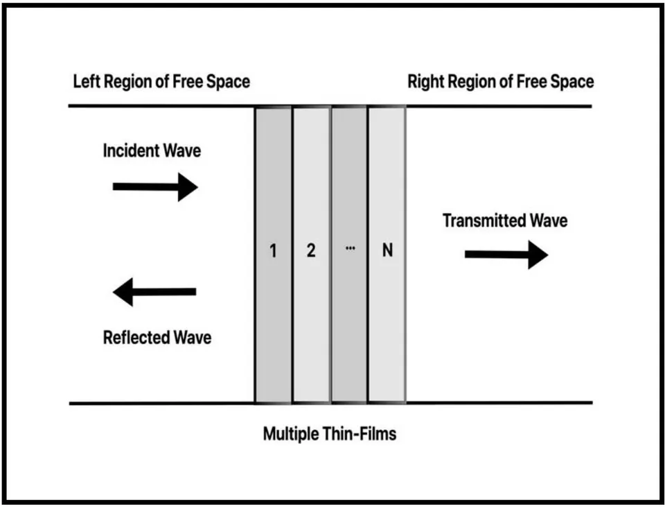
Several figures depicting thin-film structures are included in this study: Multilayer Thin Film Structure Consisting of Thin Films (1), Single Optical Thin Film (2), Single Quantum Thin Film (3), and Multilayer Thin Film Structure (6).
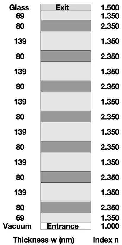
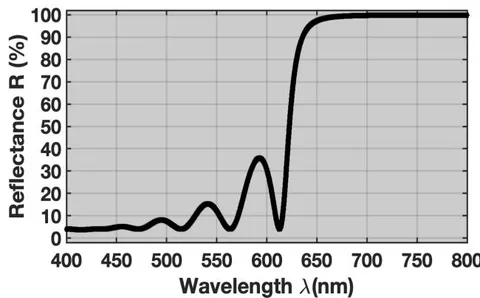
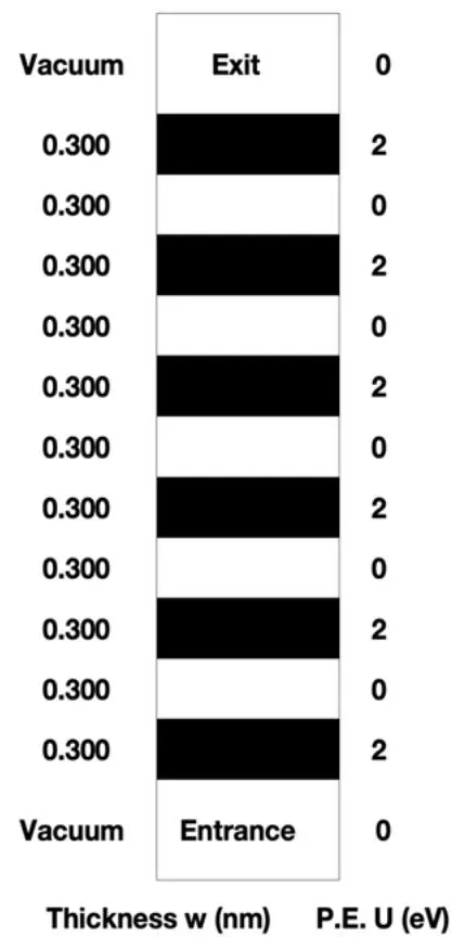
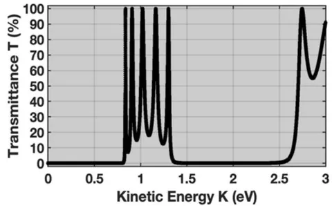
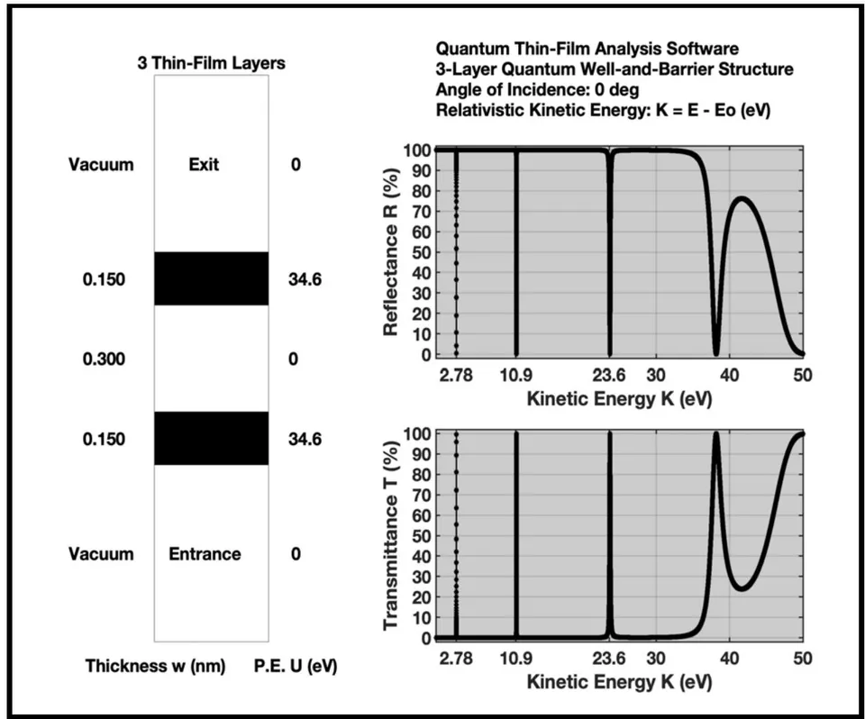
Reflectance and transmittance results are presented for a number of optical and quantum-mechanical single and multilayer thin-film structures. These include a 1-Layer Dielectric Thin Film Structure (4), 1-Layer Thin Film Quantum Barrier (5), 11-Layer High-Reflectance Mirror Structure (7), 15-Layer Long-Wave Band-Pass Optical Filter (8), 15-Layer Short-Wave Band-Pass Optical Filter (9), 15-Layer Narrow Band-Pass Optical Filter (10), 11-Layer Periodic Quantum Well-and-Barrier Structure (11), 3-Layer Well-and-Barrier Structure (12), 21-Layer Quantum Harmonic Oscillator Structure (13), and 3-Layer Nuclear Potential Well-and-Barrier Structure (14).
II. REVIEW OF THE VECTOR FIELD EQUATIONS
a) Maxwell Vector Field Equations
In our investigation of an electromagnetic wave propagating through a single dielectric optical thin film, we assumed that the dielectric was Class A. Class A dielectrics are linear, homogeneous, and isotropic dielectrics. The dielectric is characterized by a scalar permittivity and a scalar permeability . The Maxwell vector field equations in Gaussian units [1] for a dielectric material are given by
represents the electric field vector and is the magnetic field vector. The symbol represents the speed of light in free space.
b) Dirac Vector Field Equations
In our investigation of a quantum mechanical matter wave propagating through a single quantum thin film, relativistic Dirac vector field equations played an important role. In the Gaussian units references [2] and [3], these equations are given by
is defined as the upper field vector and is defined as the lower field vector. The imaginary quantity represents the square root of minus one. The constant is defined as follows:
Here represents the rest mass of the matter wave particle, its rest mass energy and is the reduced Planck's constant equal to Planck's constant divided by . Note the similarity between the Maxwell and Dirac vector field equations.
III. REVIEW OF THE WAVE EQUATIONS
a) Electromagnetic Wave Equations
From the Maxwell vector field equations, the following pair of electromagnetic wave equations for electric field and magnetic field can be easily obtained:
The quantity represents the wave propagation speed through a dielectric medium. The refractive index of the dielectric material is defined as follows:
b) Quantum Mechanical Wave Equations
Similarly, from the Dirac vector field equations, the following pair of quantum mechanical wave equations for the upper field and lower field can be obtained.
These two quantum mechanical vector wave equations have the same form as the quantum mechanical Klein-Gordon equation.
IV. REVIEW OF THE PLANE WAVE SOLUTIONS
a) Electromagnetic Plane Wave Solutions
To determine the reflection and transmission characteristics of a single optical thin film as a function of the wavelength of the incident electromagnetic wave, monochromatic plane-wave solutions [1] satisfying the Maxwell vector field equations and corresponding wave equations were employed:
The quantities and represent the maximum amplitude electric and magnetic field vectors, respectively; and are the wave vector and angular frequency of the electromagnetic wave, respectively; and represent the position vector and instantaneous time, respectively. The magnitude of the wave vector is known as the wavenumber . Substituting equations (15) back into the Maxwell vector field equations and corresponding wave equations yields the following set of equations:
and
b) Quantum Mechanical Plane Wave Solutions
Similarly, plane-wave solutions satisfying the Dirac vector field equations and the corresponding wave equations were employed to determine the reflection and transmission properties of a single quantum thin film as a function of the kinetic energy of the incident matter wave particle. That is
The quantities and represent the maximum amplitudes of the upper and lower field vectors, respectively, and and correspond to the linear momentum and total energy of the matter-wave particle, respectively. Substituting Equation (19) back into the Dirac vector field equations and corresponding wave equations yields the following set of equations:
and
V. REVIEW OF THE PLANE WAVE PROPERTIES
a) Electromagnetic Plane Wave Properties
From equations (16) and (17), we find that the vectors , , and are mutually perpendicular. That is
This electromagnetic wave is transverse. We also obtained important results for wave amplitudes.
or equivalently
where the quantities and are the admittance and impedance of the dielectric material, respectively, defined by
b) Quantum Mechanical Plane Wave Properties
From equations (20) and (21), we find that vectors , , and are mutually perpendicular. That is
This quantum-mechanical matter wave is transverse in nature. We also obtained important results for the wave amplitudes.
From the special theory of relativity [4], the quantity in equations (21) and (26) is known as the Lorentz factor. It is related to the speed of a relativistic moving particle by the following equation:
is known as the speed parameter.
VI. THIN FILM STRUCTURES
a) Single Optical Thin Film
Figure (2) depicts a single optical thin film surrounded by free space with parallel planar surfaces. The thin film has thickness and is composed of a Class A dielectric material with permittivity and permeability . Other quantities useful for characterizing thin films are the index of refraction , admittance and impedance , where
Notably, the permittivity and permeability of free space are both equal to unity when the Gaussian units are used.
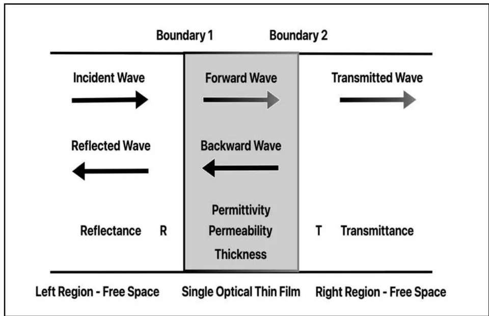
An incident electromagnetic wave, with wavelength , strikes the optical thin film at normal incidence, giving rise to both reflected and transmitted waves. Our primary goal is to determine mathematical formulae for predicting the reflectance and transmittance of the optical thin film as a function of the wavelength and quantities , , and . The fundamental equations used in the mathematical analysis are the Maxwell vector field equations.
b) Single Quantum Thin Film
Figure (3) depicts a single quantum thin film surrounded by free space with parallel planar surfaces. The only two quantities of interest in describing a quantum thin film are its thickness and the electrical potential externally applied to the thin film. The potential energy , of an electron in the presence of an electrical potential , is given by , where is the elementary charge.
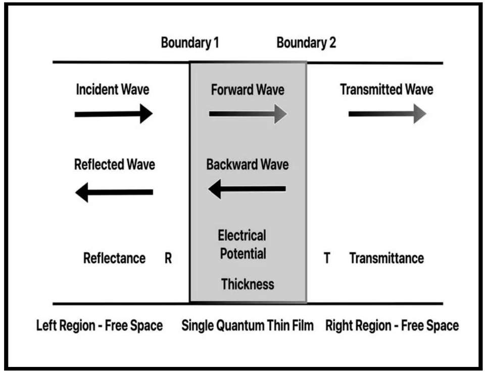
An incident quantum mechanical matter wave particle, having kinetic energy , strikes the quantum thin film at normal incidence giving rise to both a reflected and a transmitted matter wave. Our primary goal is to determine mathematical formulae for predicting the reflectance and transmittance of the quantum thin film as a function of the kinetic energy and its potential energy . The fundamental equations to be used in the mathematical analysis are the relativistic Dirac vector field equations.
VII. MATHEMATICAL ANALYSIS
a) Optical Thin Film Analysis
i. Electromagnetic Waves
As shown in Figure (2), five electromagnetic waves were considered. In the left region, we have the incident and reflected waves. Within the optical thin film, we have forward waves and backward waves. In the right region, we only have the transmitted wave. Equation (23) allows us to express the following relationship between the electromagnetic wave electric and magnetic wave amplitudes:
Left Region: Incident and Reflected Waves
Optical Thin Film: Forward and Backward Propagating Waves
Right Region: Transmitted Wave
The subscripts , and refer to the left, right and optical thin film, respectively.
ii. Optical Thin Film Boundary Conditions
Recall that the incident electromagnetic wave impinges on the thin film at a normal incidence. The electric and magnetic vectors are perpendicular (transverse waves) to the direction of wave propagation. At each of the two planar boundaries separating the various regions, the tangential components of the electric and magnetic field vectors are continuous across the boundary [1]. Mathematically, this implies that:
Boundary 2 on the Right
The phase angle , associated with the optical thin film [5] depends on three quantities: the index of refraction of the thin film, the thickness of the thin film and the wavelength of the incident electromagnetic wave. The mathematical expression for is given by
Using equations (29), (30), and (31), we can express the magnitude of the magnetic field amplitudes in terms of the electric field amplitudes. That is
Boundary 1 on the Left
Boundary 2 on the Right
From these four equations, with little algebra, we can eliminate the and fields, leaving two equations that involve the three fields and . The following ratios can be determined from the remaining two equations.
The quantities and represent the reflectivity and transmissivity of the optical thin films, respectively.
iii. Optical Thin Film Reflectivity and Transmissivity
The final mathematical formulae for the reflectivity and transmissivity of a single optical thin film are given by:
To compute the reflectance and transmittance of the optical thin films, the following equations were used.
The superscript symbol implies the complex conjugate operation.
b) Quantum Thin Film Analysis
Recall that the traditional Maxwell vector field equations (1) through (4) are similar in structure to the newly formulated relativistic Dirac vector field equations (5) through (8). Using the same mathematical analysis procedure for the single-quantum thin-film case leads to equations (42), (43), and (44) to describe the reflection and transmission characteristics of the single-quantum thin film.
Several physical quantities for the optical thin-film case must be replaced by certain physical quantities for the quantum thin-film case. A conversion table summarizing the details of changing certain classical electrodynamic quantities to relativistic quantum-mechanical quantities, is presented in Table 1.
| Dielectric Material Properties | Classical Electromagnetic Theory | Relativistic Quantum Theory | |
| Electric Field | E | ⇒ | U |
| Magnetic Field | H | ⇒ | L |
| Permittivity | 1 ≤ ε | ⇒ | (γ + 1) |
| Permeability | 1 ≤ μ | ⇒ | (γ - 1) |
| Refractive Index | n = √με | ⇒ | √γ2 - 1 |
| Admittance | Y = √ε/μ | ⇒ | √(γ + 1)/(γ - 1) |
| Impedance | Z = √μ/ε | ⇒ | √(γ - 1)/(γ + 1) |
| Thickness | 0 < w | ⇒ | 0 < w |
| Wavenumber | k = 2π/λ | ⇒ | k = Eo/ħc |
| Phase Factor | φ = knw | ⇒ | φ = knw |
Notice the wavenumber , in the relativistic quantum theory column, is the same constant defined in equation (9) and appearing in the Dirac vector field equations (7) and (8). Two examples of reflectance and transmittance graphs for a single optical thin film and a single quantum barrier thin film are presented in Figures (4) and (5), respectively.
Single Dielectric Optical Thin Film Example
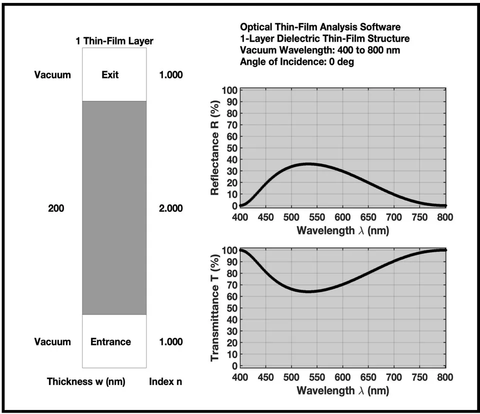
Referring to Figure (2), the left and right free space (vacuum) region's permittivity and permeability . According to Table 1, the refractive index , the admittance and the impedance for both of these free space regions as well. The optical thin film has a permittivity and a permeability . This implies the refractive index , the admittance and the impedance . The optical thin-film thickness . The wavelength of the incident electromagnetic wave was varied between to . Equations (42), (43) and (44) were used to evaluate the reflectance and transmittance as a function of the wavelength using MATLAB computer software, reference [6]. The left hand side of Figure (4) depicts the optical thin-film structure.
Single Thin Film Quantum Barrier Example
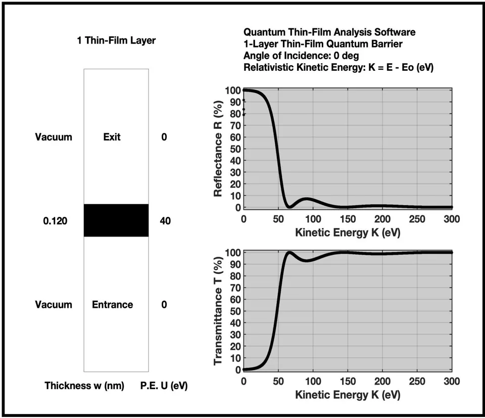
Referring to Figure (3), an electron, whose kinetic energy varies between 0 eV and 300 eV, impinges upon a single quantum barrier at normal incidence. The left and right free space region's potential energy . The potential energy of the quantum barrier and its thickness . With the help of Table 1 and equations (42) through (43), the reflectance and transmittance plots are shown in Figure(5). The Lorentz factor for each region is determined using the equation where the total energy of the electron is given by . Here or for the left, right or quantum thin-film regions. Once the Lorentz factors are determined, then the various quantities listed in the relativistic quantum theory column of Table 1, may be computed. The results presented in Figure(5) are in agreement with those presented in reference [7].
VIII. MULTILAYER THIN FILM STRUCTURES
a) Multilayer Thin Film Diagram
Figure (6) depicts a multilayer thin-film structure consisting of thin films with parallel planar boundaries. An incident electromagnetic wave or a quantum mechanical matter wave strikes a multilayer thin-film structure at normal incidence, resulting in reflected and transmitted waves. Equations for predicting the reflectance and transmittance of the multilayer thin-film structure are presented.
b) Matrix Representation
The key matrix equation for this section is given by
The 2-by-2 matrix contains all information about the thin-film structure, where
Each 2-by-2 matrix , for , is defined by
This equation indicates properties of the th thin film must be known, namely , and , the phase angle, admittance, and impedance of the th thin film, respectively. From Table 1, the admittance and the impedance are related by .
The electric-field magnitudes , and for the incident, reflected, and transmitted waves, respectively, are the elements of the wave vectors
The remaining three matrices , and are defined by
Once the matrices , , and for all values have been determined, as listed in Table 1, the reflectivity and transmissivity can be determined. Finally, the reflectance and transmittance are given by
In the following two sections, reflectance and transmittance graphs, based on numerical computer computations, are presented for a number of different optical thin-film structures as well as quantum thin-film structures. MATLAB computer software was employed for both computations and graphics.
IX. OPTICAL THIN FILM GRAPHICAL RESULTS
The reflectance and transmittance characteristics of four different multilayer optical thin-film structures are presented in this section based on the formalism of Maxwell vector field equations. Each thin film in the multilayer structure is characterized by having a constant index of refraction and thickness . For these four examples, the permeability constant and the permittivity constant .
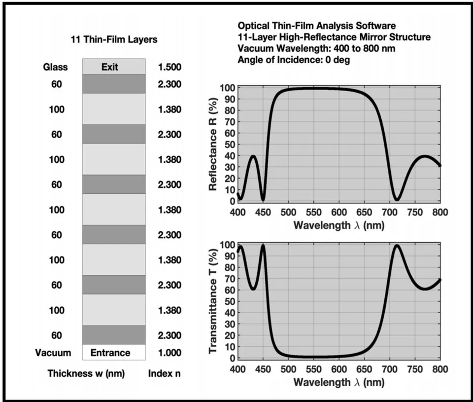
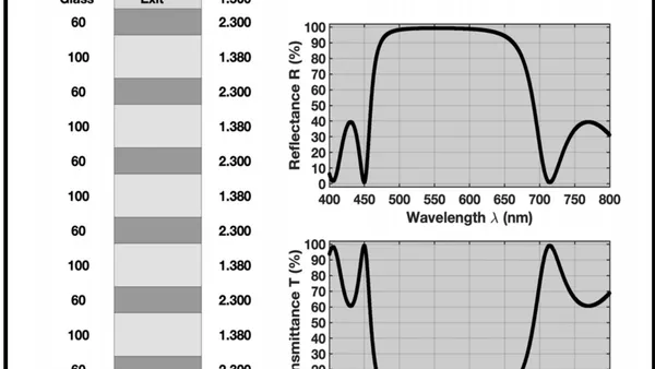
The results shown in Figure (7), correspond to light whose wavelength varies between and , incident upon an 11-layer high-reflectance mirror structure. The left portion of this figure depicts the multilayer structure physical properties. The results are in excellent agreement with those published in reference [5].
b) 15-Layer Long-Wave Band-Pass Optical Filter
Reference [5] provides an excellent discussion of band-pass optical filters. The next two examples represent long- and short-wave band-pass optical filters, respectively.
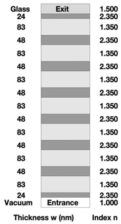
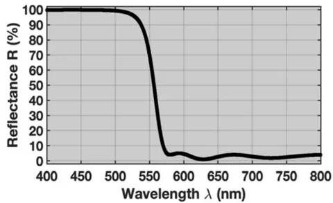
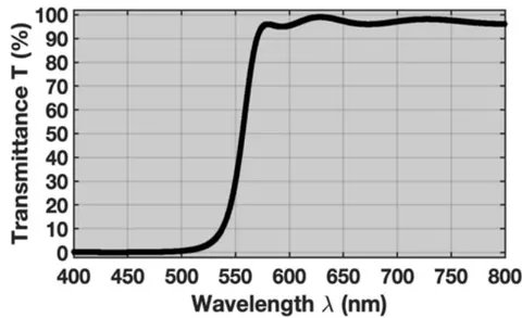
This example is that of a 15-layer long-wave band-pass optical filter as shown in Figure (8). The wavelength of the incident light was varied between and . Again, the results are in excellent agreement with those presented in [5].
c) 15-Layer Short-Wave Band-Pass Optical Filter
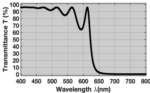
d) 15-Layer Narrow Band-Pass Optical Filter
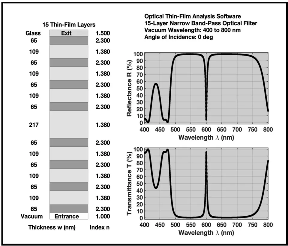
This example is that of a 15-layer narrow band-pass optical filter centered at approximately . The wavelength of the incident light was varied between and . The results shown in Figure (10) are in excellent agreement with those presented in reference [5].
X. QUANTUM THIN FILM GRAPHICAL RESULTS
The reflectance and transmittance characteristics of four different multilayer quantum wells and barrier structures are presented in this section, based on the relativistic Dirac vector field equation formalism. Each thin film in the multilayer structure was characterized by the potential energy and thickness .
a) 11-Layer Periodic Well-and-Barrier Structure
b) 3-Layer Quantum Well-and-Barrier Structure
In this example, the energy levels of a rectangular potential well are determined by casting the problem into one involving a potential well surrounded by two identical quantum barriers. Electron tunneling through the 3-layer quantum well-and-barrier structure occurs at kinetic energies corresponding to or near the energies of the quantum well.
c) 21-Layer Quantum Harmonic Oscillator Structure
In this example, the quantum harmonic oscillator problem is converted into a multilayer quantum well-and-barrier problem. The goal was to determine the energy levels of a quantum harmonic oscillator characterized by a potential energy where is the spring constant and is the mass of the attached particle.
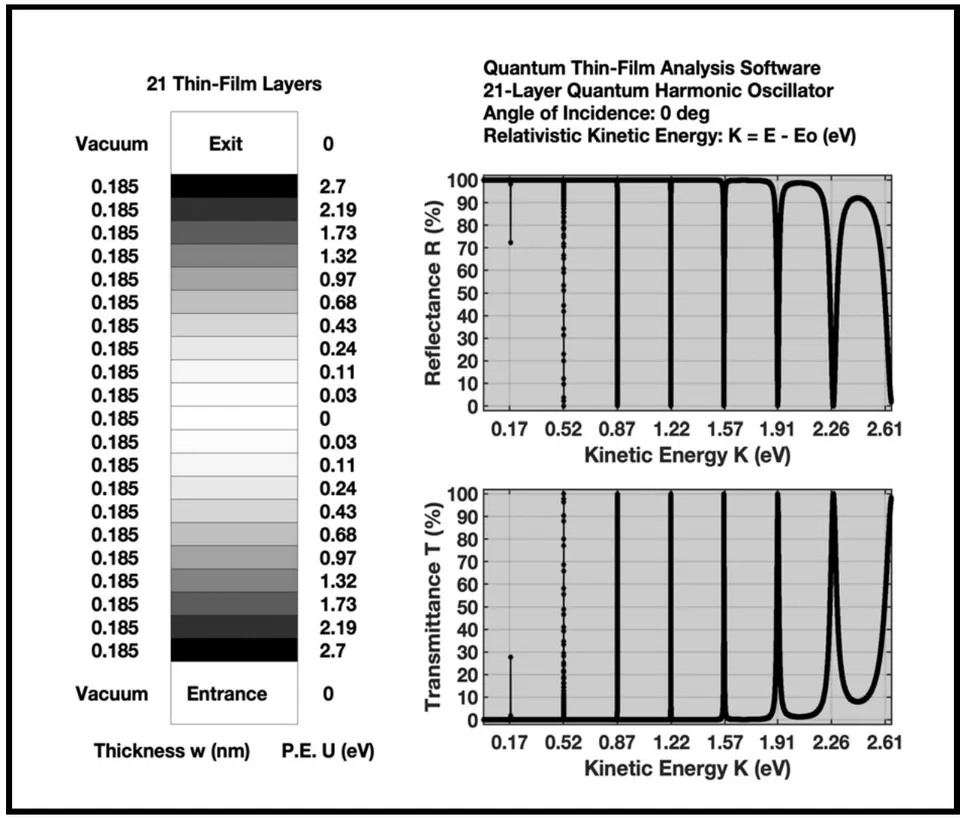
where is reduced Planck's constant. The truncated multilayer quantum well-and-barrier total width . The structure is depicted in Figure (13). The kinetic energy of the incident particle was varied between 0 eV and 2.65 eV. The eight energy levels associated with this truncated quantum well-and-barrier structure were correctly predicted, as shown in the graphs above and in agreement with the theory presented in reference [10].
d) 3-Layer Nuclear Potential Well-and-Barrier Structure
Again, the Dirac vector field equations are a set of relativistic field equations, whereas the Schrödinger wave equation is a non-relativistic equation. The next example concerns the predicted energy levels of a 3-layer nuclear potential well structure [11].
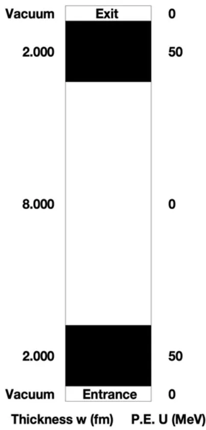
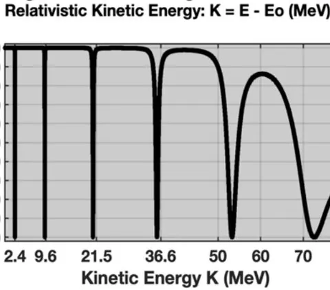
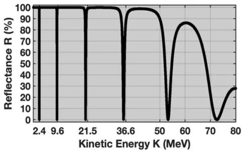
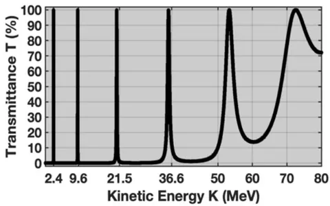
Here again the problem was converted into quantum well-and-barrier problem. This time a neutron, whose rest mass energy is 939.6 MeV, was used as the incident particle. Its kinetic energy was varied between 1 MeV and 80 MeV. At 80 MeV the neutron has a speed and a Lorentz factor of , certainly considered relativistic. The nuclear potential well has a width fm. Each of the two identical surrounding quantum barriers have a width of 2.00 fm and potential energy levels MeV. The four energy levels of the nuclear potential well were correctly predicted: 2.4 MeV, 9.6 MeV, 21.5 MeV and 36.6 MeV as shown in Figure (14). These predictions are in excellent agreement with reference [11].
XI. SUMMARY AND CONCLUSIONS
The traditional Maxwell vector field equations in Gaussian units [1] and the newly formulated relativistic Dirac vector field equations in Gaussian units [2] and [3] serve as the underlying equations for the formulation of a unified approach for determining the transmission and reflection properties of multilayer optical and quantum thin-film structures. Based on the similarity between these two sets of field equations, the formulation of a unified approach is straightforward.
In particular, using the Maxwell vector field equations describing a dielectric material, a pair of analytical equations is used to predict the reflectance and transmittance of a single thin-film layer, for the case of normal incidence of an electromagnetic wave. The reflectance and transmittance represent the probabilities that a single photon, associated with the electromagnetic wave, is either reflected or transmitted through the thin-film layer.
Similarly, using the Dirac vector field equations, a pair of analytical equations can be used to predict the reflectance and transmittance properties of a single quantum barrier in the case of the normal incidence of a quantum mechanical matter wave. Reflectance and transmittance represent the probabilities that a single particle (electron or neutron) associated with the matter wave will be either reflected or transmitted through the quantum barrier.
Upon comparing the classical electromagnetic and relativistic quantum mechanical equations for predicting reflectance and transmittance , it is clear that these equations are identical. The only difference is that certain classical electromagnetic quantities can be replaced by suitable relativistic quantum mechanical quantities. Table 1: Unified Approach Conversion Table.
The single thin-film approach has been generalized to handle multilayer thin-film structures. Using the information in Table 1, a computer program using MATLAB computational and graphics software was developed to determine the reflection and transmission characteristics of either multilayer optical thin-film structures or multilayer quantum well-and-barrier structures. Predictions based on this unified approach and computer software development were tested thoroughly. The results were compared with those published in the literature and showed excellent agreement.
Several figures depicting thin-film structures were included in this study: Multilayer Thin Film Structure Consisting of Thin Films (1), Single Optical Thin Film (2), Single Quantum Thin Film (3), and Multilayer Thin Film Structure (6).
Reflectance and transmittance results were presented for a number of optical and quantum-mechanical single and multilayer thin-film structures. These include: 1-Layer Dielectric Thin Film Structure (4), 1-Layer Thin Film Quantum Barrier (5), 11-Layer High-Reflectance Mirror Structure (7), 15-Layer Long-Wave Band-Pass Optical Filter (8), 15-Layer Short-Wave Band-Pass Optical Filter (9), 15-Layer Narrow Band-Pass Optical Filter (10), 11-Layer Periodic Quantum Well-and-Barrier Structure (11), 3-Layer Well-and-Barrier Structure (12), 21-Layer Quantum Harmonic Oscillator Structure (13), and 3-Layer Nuclear Potential Well-and-Barrier Structure (14).
Because of the similarity between the classical Maxwell vector field and relativistic Dirac vector field equations, researchers now have an alternative method for analyzing the nature of similar physical phenomena in the optical and quantum regimes.
Declarations
Author Contribution Statement: The author conceived and designed the analysis; Analyzed and interpreted the data; Contributed analysis tools and data; Wrote the paper.
Funding Statement: This study did not receive any specific grants from funding agencies in the public, commercial, or not-for-profit sectors.
Data Access Statement: Research data supporting this publication are generated in this document. All relevant data are within this paper.
No additional information is available for this study.