The dirty graphene wave has swept across the entire scientific world. And it has once again confirmed that quasi-scientific speculations without taking into account the Fundamental Laws only lead to huge waste of effort and resources. But this wave was able to arise because it was not out of nowhere. Nobel laureates, who were in a hurry to get money, simply stated what was, in principle, expected, but from the prevailing erroneous Model of Graphite. And, thus, with their ignorant “proofs” they led the research of thin graphite layers down the wrong path. The analysis carried out in this article, using the example of the SIMPLE Graphite Material and its ultra-thin layers in a congruent matrix of boron nitride, shows how it is possible to create a whole class of fundamentally new, real materials. The ideal correct structure of thin layers of rhombohedral graphite, down to mono atomically thin, can be obtained not for a freely suspended (on sticky tape) film and not due to Van der Waals forces, as graphenologists claim, but in a congruent matrix -a crystal of rhombohedral boron nitride. And a radical improvement in the properties of materials can be obtained on the basis of truly unusual properties of such graphite layers with an undamaged surface, and in no way on the basis of a graphene model that does not correspond to the real material.
## I. PREAMBLE
I feel guilty that the dirty graphene wave arose at all.
On the one hand, during half a century of work at the Academy of Sciences, I saw its degeneration and that illiterate careerists were climbing into Russian academics, who supported the nomination of also illiterate Russian specialists in adhesive tape for the Nobel Prize.
On the other hand, our employee, being the author of a handbook on graphite and nitrides published in Springer, did not even bother to look into the scientific journal of our institute, where our article with Sharupin, correcting the models of graphite and boron nitride, had long been published, but inserted an ancient, meaningless article (as the authors themselves wrote in the conclusion). So the general public had ideas about graphite from the beginning of the last century, which prompted graphenologists to childish fantasies.
And on the third hand, the energetic rogue, the late director of our very own loffe Institute, Zholes Alferov, set an example for other rogues of how to promote any nonsense for a Nobel Prize.
I have already written a lot about the fact that graphene was the name for speculations on graphite that are far from science in my popular science articles on the website of the Nanotechnology Society of Russia [1,2]. And in Wikipedia, in the article on Van der Waals forces, I also wrote that these forces, introduced for crystals formed from deeply cooled inert gases, cannot in any way be used to describe refractory crystals and for the model of a single-atom film. But graphene speculations did not arise out of nowhere - graphite, a well-known layered mineral, has been studied for a long time and at length. And it was these studies, believing that it is the monoatomic layers that slide in graphite, that Pauling used to construct a model of flat electron (sigma) orbitals that connect carbon atoms in graphite layers into hexagons [3]. Pauling, as a chemist, could not ignore the fact that the carbon atom has 4 valence electrons and introduced an additional pi-orbitals, which he assumed also connect (weakly, slipperily - blurred throughout the layer) the hexagons of different layers. But this crude model did not take into account the spatial distribution of interlayer bonds and their localization on carbon atoms. This created the illusion of their uniform distribution throughout the layer, which led to a purely theoretical misconception that the bonds between atomic layers are formed due to van der Waals forces [4]. At the same time, the compilation works of Dreselhaus [5] also did a disservice to the science of graphite.
These abstract ideas about graphite, contradicting both the known relatively small anisotropy of the Debye temperature and the fact that graphite crystals do not break at 3000 degrees, based on the primitive idea of the sliding of graphite layers (in reality, graphite flakes slide, not monoatomic layers in them) formed both the theoretical models of graphite energy bands and the drawn, free-hanging and in a vacuum monoatomic layers of graphite, called graphene. Although it is clearly visible, even in the example of a balloon, that without external support the film will shrink. It was also already known that pieces of graphite monoatomic film shrink into a ball, called fullerene. Landau's theorem also speaks about this, proving that purely one-dimensional and two-dimensional objects in a free state cannot exist. Unlike dreamers with sticky tape, we, together with B.N. Sharupin [6], who created boron nitride for the first time in the world, studied graphite pyrocrystals with different degrees of ordering of the crystal lattice. In this case, it was verified that up to pressures of $60\mathrm{kBar}$, liquid metals do not penetrate between monoatomic layers - the liquid metal enters only defects between graphite flakes. An increase in electrical conductivity along the C axis was also discovered with a high degree of ordering of graphite crystals (Fig. 1), when graphite passes from the
hexagonal phase with disordered interlayer bonds and with a translation period along the C axis equal to twice the interatomic distance into the rhombohedral phase with a strict translation period along the C axis equal to three times the interplanar distance.
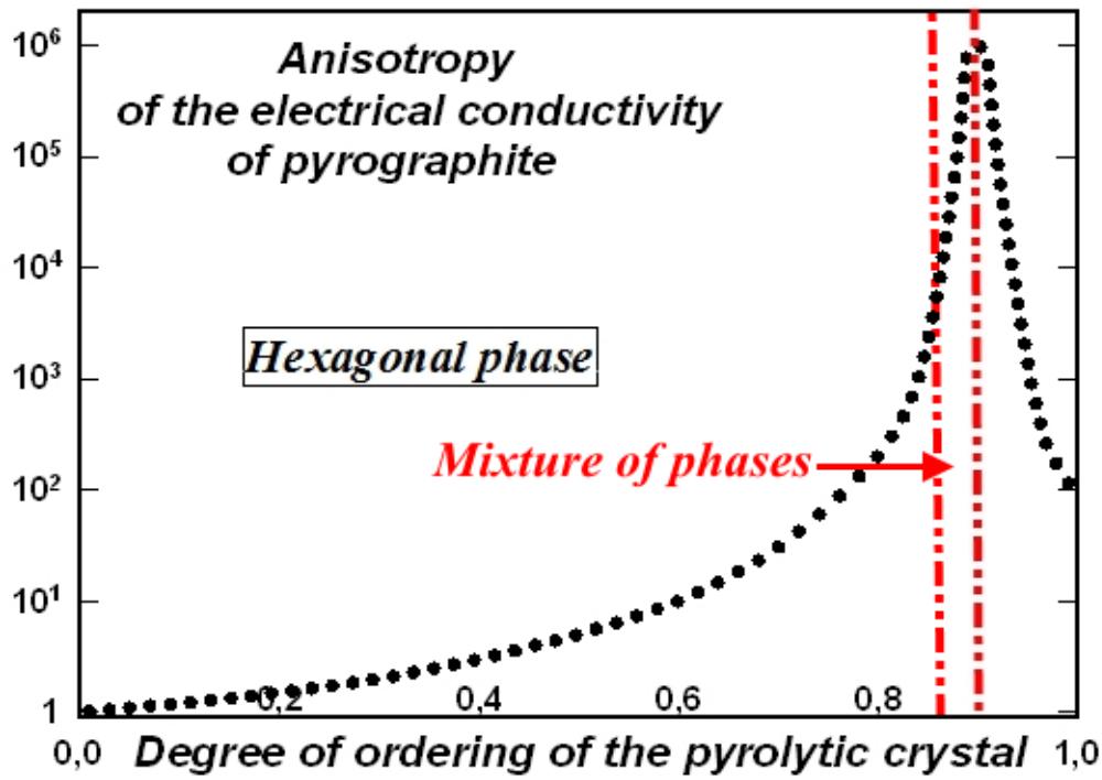 Fig. 1: Reduction of the anisotropy of electrical conductivity of graphite pyrocrystals during the transition from the hexagonal phase to the rhombohedral phase due to an increase in electrical conductivity across the monatomic layers of graphite
In this case, the degree of ordering of the crystal lattice in Fig. 1 was determined, as described earlier, by the blurring of the translation parameters, both in the plane of the hexagons and along the C axis. In parallel to graphite, pyrocrystals of its dielectric analogue, boron nitride, created by B.N. Sharupin, were studied [7]. As studies have shown, a decrease in anisotropy at a very high degree of ordering of pyrocrystals is associated not only with the ordering of their microstructure, but with the order-disorder transition in the distribution of interlayer bonds in the crystal lattice [8]. The transition from chaotically distributed interlayer bonds to strictly ordered ones determines, both in graphite and in boron nitride, the phase transition from the hexagonal phase, with a period of translation of monatomic layers along the C axis equal to twice the interatomic distance, to the highly ordered rhombohedral phase with a period of translation of monatomic layers equal to three times the interatomic distance (Fig. 2).
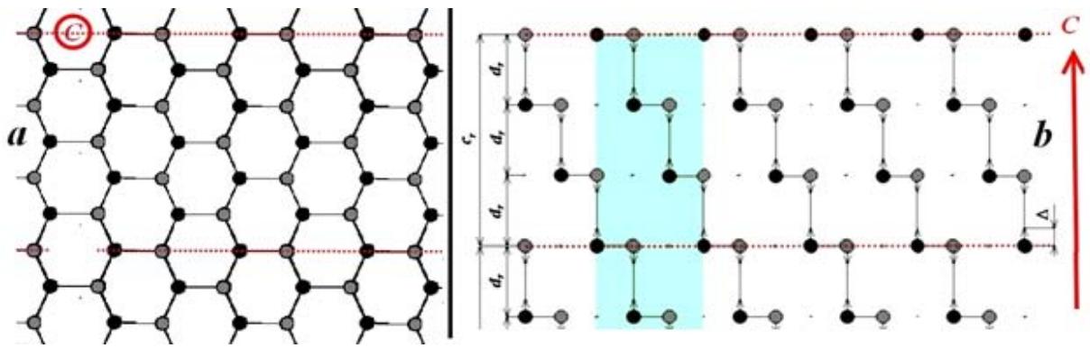 Fig. 2: Model of the crystal lattice of highly ordered rhombohedral boron nitride: a - plane perpendicular to the C axis, b - plane parallel to the C axis
At the same time, since the crystal lattice of boron nitride contains a dipole, its characteristic lattice vibrations are IR-active and the reflection spectra of boron nitride crystals clearly demonstrate strongly damped lattice oscillators in the hexagonal phase in reflection and weakly damped lattice vibrations in the rhombohedral phase in the region of the same frequencies (Fig. 3).
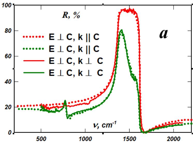
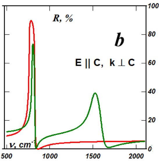 Fig. 3: Lattice oscillators in the polarization reflection spectra of rhombohedral (red curves) and hexagon al (green curves) boron nitride
In highly ordered rhombohedral boron nitride, weakly damped lattice oscillators are observed. In this case, for each polarization of IR radiation, only one, corresponding to ion oscillations in the plane of the hexagons (Fig. 2a) and ion oscillations along the C axis - perpendicular to the plane of the hexagons (Fig. 2b). And since the low-frequency edge of the oscillator corresponds to a transverse phonon and determines the rigidity of the bond between atoms in the crystal lattice, Fig. 2 shows that the interlayer bond is only one and a half times weaker than the intralayer bond, which is in full agreement with the anisotropy of the Debye temperature. But, as was shown earlier, in the rhombohedral crystal lattice, there is one interlayer bond per intralayer bond. Therefore, the rigidity of the boron nitride crystal along the C axis is only 4.5 times less than its rigidity perpendicular to the C axis, and not 1000 times, as follows from the Van der Waals forces [8].
The presence of a dipole in the boron nitride crystal lattice makes its oscillations IR-active and determines the width of the oscillator - its high-frequency edge corresponds to a longitudinal phonon that exists only in the boron nitride crystal, but the transverse phonons in the rhombohedral phases of boron nitride and graphite are close in frequency. In this case, graphite in the rhombohedral phase becomes a semi-metal with noticeable intrinsic electrical conductivity along the C axis, which, with an insignificant increase in electrical conductivity along the graphite layers, determines the drop in the anisotropy of its electrical conductivity.
The obtained absorption spectra of pyrographites (Fig. 4a) are well described by the additive contributions of two processes: $\alpha \sim (\mathrm{E} - (\Delta \mathrm{E}_1 + \mathrm{E}_{\mathrm{ph}})^2$, with the characteristic frequency $(\Delta \mathrm{E}_1 + \mathrm{E}_{\mathrm{ph}}) / \hbar = -640~\mathrm{cm}^{-1}$, where $\mathrm{E}_{\mathrm{ph}}$ is the phonon frequency, and direct allowed transitions: $\alpha \sim (\mathrm{E} - \Delta \mathrm{E}_2)^{1/2}$, with $\Delta \mathrm{E}_2 / \hbar = +1000~\mathrm{cm}^{-1}$. Considering that the maximum phonon frequency for graphite is about $1400~\mathrm{cm}^{-1}$, the obtained values of the edges of inter band transitions correspond to a band structure with a direct gap near the Fermi level of about $0.125~\mathrm{eV}$ and with an indirect anisotropic overlap of $0.25~\mathrm{eV}$ (Fig. 4b). From the above analysis it follows that with a decrease in the degree of disordering of pyrographites, the direct energy gap decreases, and the overlap of the bands increases [9].
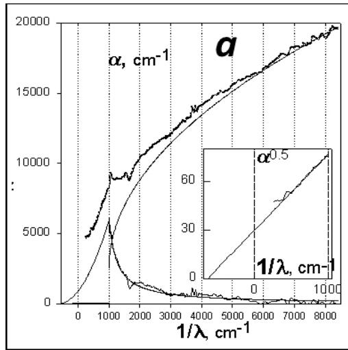
 Fig. 4: Absorption spectrum of a film of finely dispersed pyrolytic graphite-pyrocarbon (a) and a model of the band structure of graphite (b)
The presented zone model (Fig. 4b) shows that to the normal, relatively small semi-metallic (zone) electrical conductivity of graphite (ordered) along the C axis, in the direction perpendicular to the C axis - in the plane of the hexagons, due to the minimal gap between the allowed zones by momentum, there is an addition in the form of "acoustic" electrical conductivity. And this large "acoustic" addition to the electrical conductivity at very low temperatures has a small "opening threshold" (minimum voltage) corresponding to the momentum gap between the allowed states, and with increasing temperature - a large increase in electrical conductivity. This is in good agreement in a wide temperature range with the anisotropy of the temperature dependence of the electrical conductivity of graphite, which manifests itself for the plane of hexagons in its purely semiconductor growth up to $800\mathrm{C}$ and in its metallic decline at a higher temperature (Fig. 5, above). Although, as experiments on high-temperature annealing of highly ordered rhombohedral nitride samples have shown, during annealing there is a phase transition to the hexagonal phase and a characteristic change in the lattice oscillators (Fig. 3). The electrical conductivity along the C axis demonstrates a continuous exponential growth with increasing temperature (Fig. 5, below), which is determined, in full accordance with the model of the band structure of graphite presented in Fig. 4, by the increasing contribution of phonons to indirect transitions.
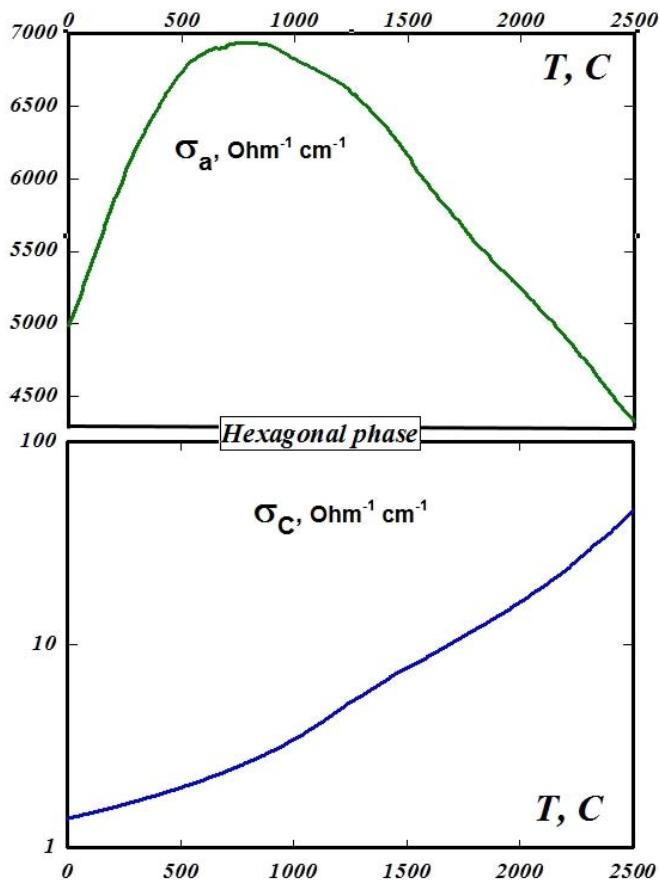 Fig. 5: Temperature dependences of the specific electrical conductivity of ordered hexagonal graphite in the plane of the hexagons (a - from above) and along the C axis (from below)
Since the crystalline structures of graphite and boron nitride are similar, it seemed possible to grow graphite layers in boron nitride and boron nitride layers in graphite. Samples of graphite with boron nitride were analyzed for the purpose of obtaining composite thermoelectric material, but in the obtained non-order composite samples, only the diffusion thermoelectric mechanism operates and the thermoelectric figure of merit, in accordance with the theory of flow in composites, did not increase significantly compared to the low thermoelectric figure of merit of pure graphite.
But since the parameters of the crystal lattices of the rhombohedral phases of boron nitride and graphite are very close, the highly ordered boron nitride of the rhombohedral phase is an ideal environment (support) for the existence of atomic-thick graphite layers. Boris Nikolaevich Sharupin grew crystals of highly ordered boron nitride containing very thin graphite layers [9, 10]. The samples were slightly cloudy when viewed through the light, since the thinnest graphite layers in boron nitride were in the form of millimeter-diameter spots. Individual thin layers of graphite naturally transmitted visible light, but since the real part of the permittivity of graphite is much greater than its imaginary part, then in aggregate, due to the interference of reflections of the thinnest layers of graphite, they give a mirror metallic reflection of visible light from the plane of the crystal, perpendicular to the C axis and practically did not reflect visible light from the plane parallel to the C axis - they were completely black for any polarization (Fig. 6). This led to a gigantic spatial dispersion in the visible region of the spectrum. As shown in Fig. 6, in the IR range, the lattice peaks of reflection of boron nitride with graphite inclusions with polarization perpendicular to the C axis are practically independent of the orientation of the wave vector (curves 4 and 5). And the anomalously large "silver" reflection in the visible range of the spectrum of boron nitride samples with graphite inclusions from the plane perpendicular to the C axis (Fig. 6, curve 4) and, thus, the giant spatial dispersion (Fig. 6, curve 5) are associated with a powerful diffraction maximum of reflection in the ultraviolet region of the spectrum, which, in frequency, corresponds to local plasma oscillations in graphite patches with a diameter of about $50\mathrm{nm}$.
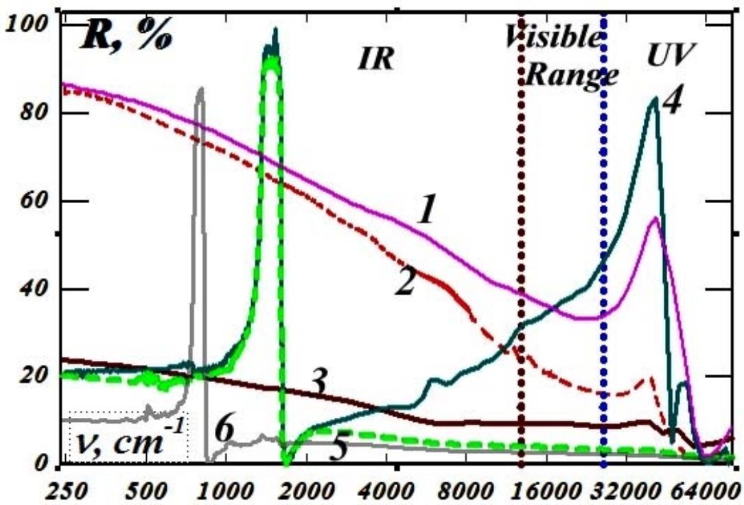 Fig. 6: Polarization spectra of reflection from different faces of highly ordered graphite pyrocrystals and highly ordered boron nitride pyrocrystals with embedded thin graphite layers:
- 1 - graphite, E$\bot$C, k$\|C$, 2 - graphite, E$\bot$C, k$\bot$C, 3 - graphite, E$\|C$, k$\bot$C, - 4 - BN, E$\bot$C, k$\|C$, 5 - BN, E$\bot$C, k$\bot$C, 6 - BN, E$\|C$, k$\bot$C.
So, millimeter spots of graphite embedded in boron nitride consist of smaller nanoflakes of antigraphene - rhombohedral graphite with a minimum thickness equal to three times the interatomic distance. The large (approaching $100\%$ ) height of the diffraction reflection peak indicates a very high electron mobility along the graphite layer in the spot. Such a giant spatial dispersion was first discovered in the IR region in disproportionate quasicrystals of higher manganese silicide [11]. But boron nitride samples with graphite
interlayers clearly demonstrated it in visible light: with polarization of the electric vector perpendicular to the C axis, a specular "silver" reflection from the plane of the crystal perpendicular to the C axis and complete non-reflection of visible light with the same polarization from a plane parallel to the C axis. This allowed us to understand that giant spatial dispersion cannot be described by the Landau smallness parameter and that these observed giant effects are described by models that are borderline between optical and radio engineering - waveguide models. And these models describe, taking into account the scale of the embedded graphite spots in boron nitride and the gigantic spatial dispersion of boron nitride with graphite.
In addition, a relatively small but significant spatial dispersion is also observed in samples of highly ordered graphite (Fig. 4, curves 1 and 2) and also with the manifestation of a characteristic peak of ultraviolet reflection. Previously, it was associated with interband transitions in graphite, which is very strange with a semimetallic overlap of energy bands. But judging by the spectra given, the graphite layers themselves consist of tightly folded 50 nano-flakes of antigraphene, electrically and mechanically contacting along the boundaries and forming packets of graphite layers with thicknesses of about $200\mathrm{nm}$.
## II. CONCLUSION
Thus, the two-sided crystalline support of thin graphite layers by the crystal lattice of rhombohedral boron nitride congruent to graphite allows obtaining unusual, but real characteristics of ultra-thin layers of rhombohedral graphite - antigraphene. With one-sided application of graphite on crystals of rhombohedral boron nitride, even on the surface perpendicular to the C axis, resulted in amorphous graphite films. That is, the break of interlayer bonds and one free surface of graphite is sufficient for the amorphization of the graphite film. Naturally, one can expect even greater amorphization of thin graphite films grown on other substrates that are poorly matched in crystal structure.
### APPENDIX
Highly ordered pyrocrystals of boron nitride with embedded thin layers of graphite were subjected to ultra-high pressure by explosion in a high-pressure chamber and thus transferred to the cubic phase (Fig. 7a).
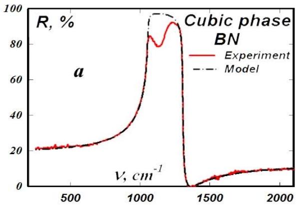
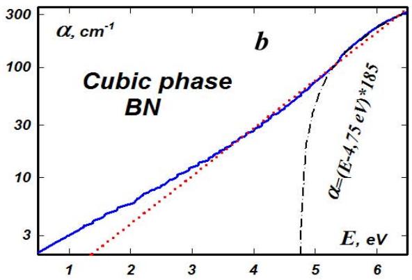 Fig. 7: Characteristic lattice oscillator of cubic boron nitride (a) and the spectrum of its absorption coefficient (b)
Uniformly weakly doped with carbon, greenish transparent crystals were obtained, the absorption spectrum of which corresponded to interband transitions with a band gap width of approximately 4.75 eV (Fig. 7b). The crystals had very high hardness and strength. Their wear resistance was almost an order of magnitude greater than that of diamond.
Generating HTML Viewer...
References
11 Cites in Article
Stanislav Ordin Website of the Nanotechnology Society of Russia.
Stanislav Ordin Website of the Nanotechnology Society of Russia.
Linus Pauling (1947). X-Ray Crystallography and the Nature of the Chemical Bond.
F Bassani,G Pastori-Parravicini (1983). Electronic states and optical transitions in solids.
M Dresselhaus,G Dresselhaus (1981). Intercalation compaunds of graphite.
B Sharupin (1976). Structure and properties of boron pyronitride.
S Ordin,B Sharupin,M Fedorov (1998). Normal lattice vibrations and the crystal structure of anisotropic modifications of boron nitride.
S Ordin,A Osmakov,V Rumyantsev,E Tupitsina,A Shelyh (2003). Real Structure Andtransition Of The Order-Disorder Type Inmodifications Of Pyrolytic Born Nitride.
S Ordin C & BN-Foundation for Atomic-Crystalline Orbitals.
S Ordin,A Osmakov,V Rumyantsev,E Tupitsina,A Shelyh (2000). Features of an electronic spectrum and a microstructure of graphite, IX National conference on growth of crystals (NCCG 2000).
S Ordin (2011). Giant spatial dispersion in the region of plasmon-phonon interaction in one-dimensionalincommensurate crystal the higher silicide of manganese (HSM).
No ethics committee approval was required for this article type.
Data Availability
Not applicable for this article.
How to Cite This Article
Dr. Stanislav V. Ordin. 2026. \u201cAnti-Graphene\u201d. Global Journal of Science Frontier Research - A: Physics & Space Science GJSFR-A Volume 25 (GJSFR Volume 25 Issue A6): .
Explore published articles in an immersive Augmented Reality environment. Our platform converts research papers into interactive 3D books, allowing readers to view and interact with content using AR and VR compatible devices.
Your published article is automatically converted into a realistic 3D book. Flip through pages and read research papers in a more engaging and interactive format.
The dirty graphene wave has swept across the entire scientific world. And it has once again confirmed that quasi-scientific speculations without taking into account the Fundamental Laws only lead to huge waste of effort and resources. But this wave was able to arise because it was not out of nowhere. Nobel laureates, who were in a hurry to get money, simply stated what was, in principle, expected, but from the prevailing erroneous Model of Graphite. And, thus, with their ignorant “proofs” they led the research of thin graphite layers down the wrong path. The analysis carried out in this article, using the example of the SIMPLE Graphite Material and its ultra-thin layers in a congruent matrix of boron nitride, shows how it is possible to create a whole class of fundamentally new, real materials. The ideal correct structure of thin layers of rhombohedral graphite, down to mono atomically thin, can be obtained not for a freely suspended (on sticky tape) film and not due to Van der Waals forces, as graphenologists claim, but in a congruent matrix -a crystal of rhombohedral boron nitride. And a radical improvement in the properties of materials can be obtained on the basis of truly unusual properties of such graphite layers with an undamaged surface, and in no way on the basis of a graphene model that does not correspond to the real material.
Our website is actively being updated, and changes may occur frequently. Please clear your browser cache if needed. For feedback or error reporting, please email [email protected]
Thank you for connecting with us. We will respond to you shortly.