

I. INTRODUCTION
As more and more cellular communication services are developed in recent mobile terminals, the multi-mode multi-band power amplifiers (PAs) is required to cramp multiple bands into a single front end[1-3]. Besides, to accommodate higher data rate of the leading WCDMA and LTE signals and extend the battery life of the handsets, high linearity and efficiency are as two most stringent specifications for the design of modern broadband PA [4,5]. Generally, the cellular PA is designed to operate with significant back-off for high linearity, but at the same time, this will decrease the power efficiency remarkably [7]. Therefore, various techniques have been presented for efficiency improvement[8-11]. This work, based on cost and integration considerations, introduces a novel broadband two-stage PA architecture which can minimize the degradation of linearity and efficiency, and at the same time, satisfy the system gain requirement. Furthermore, a two-chain parallel-amplifier structure is simultaneously realized to improve the power added efficiency (PAE) while the PA is operating in back-off by disabling one of the chains.
II. CIRCUIT ARCHITECTURE CONSIDERATIONS
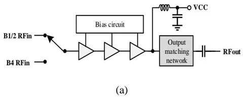
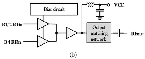
Figure1. (a) depicts a wideband three-stage PA structure. With this configuration, the system gain specification of 27dB is extremely easy to be achieved even though the insertion loss (IL) of the input switch is around 1.5 dB while the linearity and efficiency would be degraded owing to the extra stage and dc consumption. To improve the PA's linearity and efficiency, two-stage solution seems to be a better choice, however, it is difficult to satisfy the gain requirement in wideband system when only employing two-stage PA architecture with 1.5dB IL of input switch. If there is a two-stage PA solution where the input switch can be removed, then it is possible to meet the gain spec for LTE/WCDMA systems. Based on this idea, we presents a two-stage architecture with switchable driver stage, as shown in Figure.1 (b), the input of the first driver stage is connected to the Band1/2 RF input pin while the input of the second one is linked to Band 4 RF input pin, both outputs are connected to the input of the second power stage. Depending on the logic voltage level applied to the bias circuits, one of the two switched driver stages is activated for different RF input paths. This solution can not only help with the linearity and efficiency enhancement due to the absence of additional stage, but also reduce losses and improve integration as an input switch using extra GaAs pHEMT or SOI process is not required anymore.
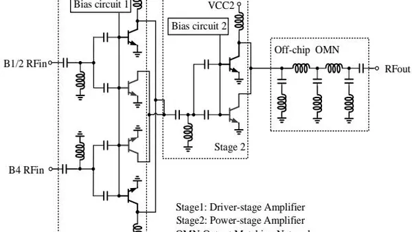
Furthermore, in view of the trade-off between efficiency and linearity, a Mid-Class AB operation is selected for the first stage (driver stage) of the presented PA, whereas a Deep-Class AB dc bias is set for the second stage (power stage). Nonetheless, even with this arrangement, the efficiency of the PA decreases as the input signal decreases in power. At these lower power levels, the PA's operating points are lowered further away from its saturation point, which leads to severe degradation of the PAE. To achieve high efficiency over a wide range of input power level, a two-stage broadband PA architecture with switchable driver-stage amplifier adopting dual-chain strategy have been developed, as shown in Figure.2. Either driver stages or power stage is composed of two-chain hetero-junction bipolar transistor (HBT) amplifiers with identical emitter areas. The two driver-stage amplifier chains for Band1/2 and Band4, respectively, have a same emitter area of and , and the two power-stage amplifier chains have a same emitter area of . In the high-power mode (HPM), two-chain HBT amplifiers are activated for high output power and the PA can obtain a P1dB of 28dBm, while for the low-power mode (LPM), only the main-chain amplifiers are enabled to achieve a P1dB of 17dBm and the aided-chain ones are disabled to reduce the bias voltage and quiescent current, and thus benefitting the efficiency improvement in the presence of low input power level.
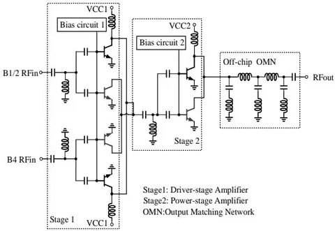
In addition, at wo-section LC low-pass filter (LPF) type network is utilized for output matching to realize broadband, and a second harmonic traps are merged into the output matching network to achieve better harmonic suppression performance.
III. FABRICATION AND MEASUREMENT
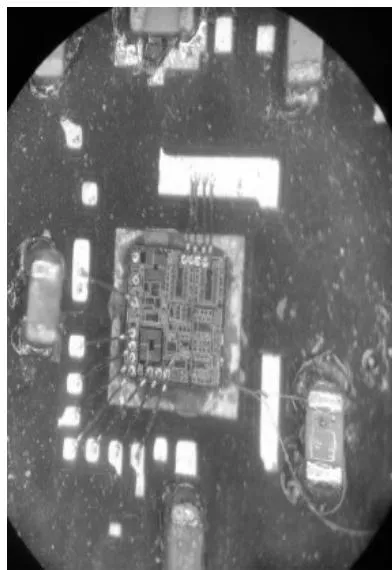
Figure. 3 illustrates the micrograph of the fabricated PA module with a size of , which in cludesa PA die with the presented two-stage dual-chain strategy in an In GaP/Ga As HBT process.
The measured linear Gain (S21) in the high power and low power modes are plotted in the Figure.4. Over the frequencies ranging from 1.7 to 2.0GHz, the PA obtains S21ranging from27.7 to 29.2dB. It can be well observed that the presented two-stage solution with switchable driver stages is able to satisfy the system gain requirement.
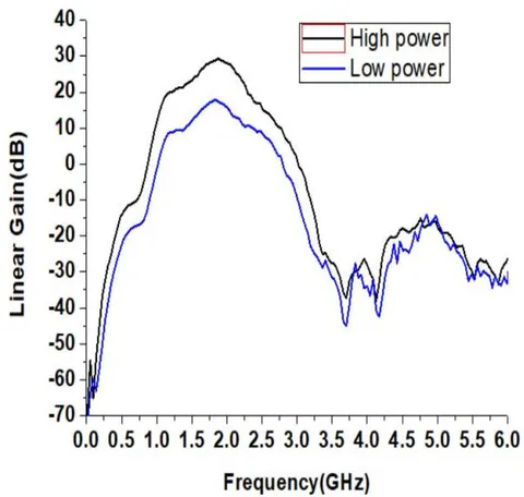
Figure 5: shows the measured output power in the high power and low power modes at 1.9GHz. At the input power (Pin) of 1dBm in the HP M and LPM, he PA gains an output power of 28.1 and 17.6dBm, respectively.
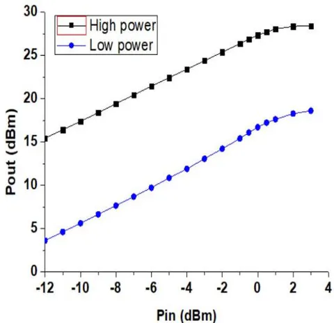
Figure. 6 describes the measured owner gain for the two modes at 1.9GHz. At the output power (Pout) of 28dBm in the HPM, the PA delivers the power gain of 27.05dB, while in the LPM, the power gain of 16.7dB is realized at the Pout of 17dBm.
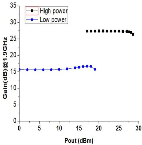
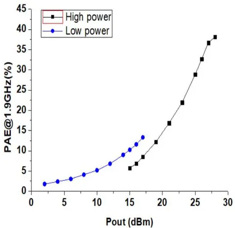
Figure 7: illustrates the measured PAE performance or responding to the different power modes at 1.9GHz. The PA delivers achieves the PAE of 38.15% at the output power (Pout) of 28dBm in the HPM, where the PAE of 13.3% is obtained at the Pout of 17dBm in the LPM. These results indicate around 4.5-5% superior PAE with the new dual-chain PA strategy, in contrast to the traditional single chain one only with HPM.
Lastly, aquiescent current (Icq) of roughly80mA for HPM and 20mA for LPM have been gained with continuous-wave power measurement. The presented PA module reveals favorable and competitive efficiency performance in the broadband WCDMA/LTE handset applications.
IV. SUMMARY
A two-stage dual-chain In GaP/Ga As HBT power amplifier module with switchable driver stages is implemented and demonstrated for multi band multi mode WCDMA and LTE handsets applications. The wideband PA module shows a38% of PA Eat 28dBm output power, and 13% of PAE at 17dBm output powerat1.9GHz, which demonstrating that the presented architecture benefits the power usage efficiency improvement of the PA when operating in the back-off.
ACKNOWLEDGMENTS
The authors wish to acknowledge all the faculty staffs in GDUT for their sincerely assistance and support to this work.