


1. Introduction
Yield and cost pressure are pushing flagship semiconductor programs toward chiplet and multi-die architectures. Smaller dies yield better than one large monolithic die, and mixing process nodes within a package lets cost track function more precisely than a single-node design allows. That much is well established. What is far less examined is what verifying a multi-die package actually demands of validation infrastructure—cross-die protocol conformance, package-level electrical and thermal interaction, and staged bring-up sequencing all draw on emulation capacity in ways a monolithic-SoC program simply never had to plan for.
Programs that size emulation capacity by extrapolating from a prior monolithic generation’s footprint tend to find out too late that the extrapolation was wrong. Compile complexity and partitioning cost scale with cross-die interface count, not merely with aggregate transistor count (a distinction that linear extrapolation methods, by construction, cannot capture). A shortfall discovered this way is rarely just a budget problem. It surfaces during multi-die bring-up, which is usually the stage of a flagship program with the least schedule slack left to absorb it.
This article takes a specific position, not a general one. Validation capacity should be planned as an explicit capital and organizational line item from the point of architectural definition—sized against die count, cross-die interface count, and protocol complexity, rather than against a prior generation’s emulator-hours-per-transistor history. That single change in what capacity is sized against, this article contends, changes both the capital outcome and the risk profile of the program.
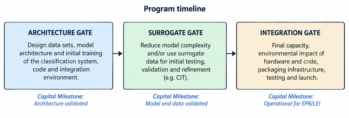
The contribution here is a staged three-gate capacity-planning framework anchored to milestones flagship programs already track: an architecture-gate sizing pass early in program definition, a subsystem-gate reforecast once per-die RTL stabilizes, and an integration-gate provisioning commitment immediately ahead of multi-die bring-up. The framework is grounded in capacity-governance and capital-planning experience directing large emulation estates supporting flagship mobile and extended-reality (XR) SoC programs (a background in capital governance and capacity architecture, not in chiplet package physical design or die-to-die circuit engineering, and the argument stays within that boundary throughout).
2. Literature Review
Chiplet validation-capacity planning sits at the intersection of three literatures that rarely cite one another directly, and reading them together is where the gap in current thinking becomes visible.
Multi-field-programmable gate array (FPGA) emulation-capacity literature carries the most direct weight for the argument developed in this article, and it is taken up first for that reason. Large FPGA-based logic emulation systems face documented scaling difficulties as design size and interconnect density grow [1], and the choice of inter-FPGA interconnect topology affects both achievable operating frequency and routing time substantially—hybrid topologies deliver routing-time improvements on the order of roughly two to nine times over baseline configurations, depending on the specific topology and design [2]. None of this research was written with chiplet integration in mind. Its implication for chiplet programs is nonetheless direct: capacity and partitioning cost sensitivity documented for monolithic multi-FPGA systems only compounds once cross-die interfaces are added on top.
Chiplet cost and yield economics is the thinnest of the three literatures, though what exists is telling. Quantitative cost modeling shows that partitioning a design into multiple smaller dies can materially improve yield-adjusted cost outcomes relative to a single large die [3]. Universal Chiplet Interconnect Express (UCIe)-class research demonstrates bandwidth density reaching several thousand gigabytes per second per square millimeter at fine bump pitches, alongside die-to-die link power figures that fall as pitch shrinks [4]; commercial EDA tooling built for single-die design, meanwhile, does not adequately support chiplet-based architectures [5], a tooling-maturity gap with a direct capacity consequence, since immature tooling tends to inflate compile and partitioning effort well beyond what an early capacity estimate would assume. A parallel literature on advanced-packaging challenges reinforces the same point from the physical-integration side [6]. Pre-silicon verification is not a marginal share of total design cost; it accounts for close to seventy percent of total design effort and cost in modern digital systems [7]. Design-cost escalation data reinforces why the partitioning argument has traction: advanced-node design cost has grown into the hundreds of millions of dollars, with next-generation nodes projected considerably higher still, and at least one documented industry case shows chiplet-based development reducing overall development cost meaningfully against a monolithic equivalent [8]. What is largely absent from this literature is any accounting for validation-capacity cost as a modeled variable. Yield and design-cost avoidance dominate the economics discussion; verification infrastructure does not appear in it at all. That silence is the gap this article is written to address.
Chiplet architecture and interconnect research fills out the third strand, and it is the most physically concrete of the three. Energy- and thermal-aware mapping heuristics for 2.5D integration report meaningful reductions in inter-chiplet communication energy [9], and multi-objective optimization approaches extend this to joint communication-and-temperature tradeoffs [10]. Processing-in-memory chiplet encapsulation work illustrates how tightly interconnect bandwidth and packaging choice are coupled [11], and dedicated thermal-interaction studies of 2.5D chiplet packages show that cooling strategy materially changes achievable power density [12]. Broader architectural surveys catalog interconnect and integration methodologies at length [13], [14], and design-space-exploration toolchains for inter-chiplet interconnects demonstrate that this exploration can now happen orders of magnitude faster than cycle-level simulation, at a modest accuracy cost [15]. Hardware-identifier and traceability research raises a related but distinct concern—provenance and counterfeiting risk specific to multi-die packages [16]—and bottom-up die-to-die interconnect optimization work shows that PHY-level latency reductions do not translate one-to-one into system-level transaction-latency gains [17]. Bare-die selection, reliability, and known-good-die screening research [18] and 3D-integration performance studies [19] round out the physical-layer picture, while on-die impedance-sensing techniques for chiplet and interposer verification [20] point toward emerging test methods built specifically for multi-die structures. None of this literature, across all three strands, treats validation capacity as a planning variable in its own right—it is architecture, packaging, and interconnect research, not capacity-economics research, and that gap is precisely what this article addresses.
| Cost Driver | Monolithic SoC | Chiplet-Based SoC |
|---|---|---|
| Die / interface count | Single die; internal interfaces only | Multiple dies; cross-die interfaces scale sub-linearly with capacity need |
| Protocol verification scope | Single protocol domain per interface class | Cross-die protocol stacks (e.g., UCIe-class) added on top of internal protocols |
| Package-level bring-up stages | Not applicable | Staged multi-die bring-up; package-level electrical/thermal interaction testing |
| Compile / partitioning complexity | Scales with aggregate transistor count | Scales disproportionately with cross-die interface count, not transistor count alone |
| Capacity-planning lead time | Single estimate near architecture freeze | Requires staged reforecast as per-die RTL and integration risk evolve |
3. Methodology / Capacity-Planning Framework
How should emulation capacity be sized when per-die RTL is still immature and multi-die integration risk is not yet fully known? The framework below answers this in three stages rather than one, because a single upfront estimate cannot absorb the uncertainty that characterizes early chiplet program definition. Each stage attaches to a milestone flagship organizations already track, deliberately—a framework demanding a new governance layer is far less likely to survive contact with an existing program-management structure than one that rides on checkpoints already in place.
Architecture-Gate Sizing. At architectural definition, before per-die RTL exists in any mature form, an early capacity estimate is built from three inputs: die count, cross-die interface count, and protocol complexity per interface, assessed qualitatively as low, moderate, or high based on interface stack depth and the number of distinct protocol domains crossing each die boundary. This estimate is meant to be directional, not precise. Its function is to establish a capital reservation early enough that emulation-asset procurement, which for large emulator platforms carries multi-quarter lead time, does not end up competing for budget cycles after the architecture is already locked.
Subsystem-Gate Reforecast. Once per-die RTL stabilizes at the subsystem level, the architecture-gate estimate is reforecast against observed compile turnaround and RTL partitioning behavior for each die. Program history across successive emulation-platform generations provides the empirical basis for this adjustment. One complication worth flagging here: subsystem RTL for different dies in the same package rarely stabilizes on the same schedule, and a reforecast run against a partially stabilized set of dies will understate compile-turnaround growth for the dies still in flux (a limitation the framework does not fully resolve, and one that requires judgment rather than a formula). This gate is where architecture-gate assumptions meet real RTL behavior for the first time, and where corrections are cheapest to make.
Integration-Gate Provisioning. Immediately ahead of multi-die bring-up, a final capacity commitment is made. This gate accounts for package-level interaction testing, staged bring-up sequencing across dies, and the compile-turnaround load of full-system cross-die scenarios rather than per-die subsystem tests alone. Provisioning at this gate exists specifically to avoid one failure mode: a capacity shortfall surfacing only after multi-die bring-up has already started, when remediation options are narrowest and schedule elasticity is close to zero.
Across all three gates, one qualitative relationship holds consistently. As die count and cross-die interface complexity rise, required emulator capacity and compile turnaround grow faster than simple linear extrapolation from monolithic-SoC history would predict—a pattern broadly consistent with documented interconnect-topology and partitioning-cost sensitivity in multi-FPGA emulation systems [1], [2]. This is not a precise growth curve. It is a planning heuristic, and organizations should treat it as such.
4. Results / Case Findings
The findings below come from the author’s own capacity-planning and capital-governance work directing emulation infrastructure across four flagship SoC generations. They are labeled Author’s primary research data throughout, distinct from the externally cited figures elsewhere in this article.
Capacity growth under staged planning. A staged capacity-planning initiative applied to a next-generation emulation platform (RUMI5+) achieved planning toward approximately double the system capacity of the prior platform generation, without a proportional rise in capital outlay. This outcome traces to sizing capacity against projected multi-die and subsystem complexity at the architecture-gate stage, rather than against the prior platform’s raw emulator-hours history. It is worth being precise about what this figure does and does not show: it reflects one platform transition inside one organization, not a general growth law, and it should be read as a case finding rather than a benchmark.
Virtualization serves as a capacity lever, not just a capital lever. System-level virtualization, enabling multiple concurrent users per physical emulation system, produced a reduction in Video-domain capital requirements from approximately $4 million to approximately $1 million. The more interesting part of this finding may not be the dollar figure itself. It shows that capacity discipline is not only about acquiring hardware ahead of need; it is about architecting utilization of hardware already owned—a lever that linear-extrapolation planning tends to miss entirely, since that approach treats capacity as an acquisition problem rather than a utilization-architecture problem.
Vendor negotiation as part of the capacity discipline, not separate from it. Structured vendor negotiation, run as part of a broader capital-governance program covering FPGA-based emulation hardware procurement, achieved an approximate 30 percent reduction in FPGA costs and associated capital savings of approximately $30 million. This finding earns its place here because it undercuts a common assumption: that capacity sizing and vendor economics are separate workstreams. They are not. A capacity framework with sound technical sizing logic will still oversize its capital ask if it ignores vendor-cost dynamics.
Set against external evidence, these program-level findings sit alongside documented industry patterns showing persistent scaling and cost pressure in FPGA-based emulation systems as design complexity grows [1], and topology-dependent routing-time and frequency effects in multi-FPGA systems [2]. Together, the author’s findings suggest staged, milestone-linked capacity governance can outperform linear-extrapolation planning on both capital efficiency and technical adequacy—a comparison that remains qualitative, and one for which no controlled counterfactual program exists to test directly.
| Dimension | Linear-Extrapolation Planning | Staged Validation-Driven Planning (this framework) |
|---|---|---|
| Capital outlay approach | Single upfront estimate from prior monolithic-generation emulator-hours history | Staged: architecture-gate estimate, subsystem-gate reforecast, integration-gate commitment |
| Capacity headroom at integration gate | Frequently under-provisioned; gap discovered at bring-up | Sized against observed per-die RTL and cross-die interface behavior before bring-up |
| Incidence of late-discovered shortfalls | Higher; surfaces when schedule elasticity is lowest | Reduced; capacity assumptions tested and corrected at subsystem gate |
| Illustrative case outcomes (author’s primary data) | Not applicable (counterfactual) | 2x capacity via staged RUMI5+ planning; Video-domain capital reduced $4M to $1M via virtualization; 30% FPGA cost reduction ($30M savings) via structured vendor negotiation |
5. Discussion
Does validation-driven capacity planning change what emulation infrastructure is, organizationally? The findings above suggest it does. Under linear extrapolation, capacity is decided once, early, and revisited only when a shortfall forces an unplanned request. Under the staged model proposed here, capacity becomes a governed variable revisited at three defined points—which turns an infrastructure request into a program-risk decision, made with roughly the same rigor a program applies to schedule or budget decisions.
Does chiplet cost-and-yield literature already account for this risk? It does not appear to, at least not explicitly. That literature makes a strong case that partitioning a design into multiple dies improves yield-adjusted cost outcomes [3], and that design-cost escalation at advanced nodes makes partitioning increasingly attractive [8]. What it does not examine is whether the validation-capacity cost required to realize those benefits offsets some portion of the projected savings. Pre-silicon verification already represents close to seventy percent of total design effort and cost for monolithic SoCs [7]; multi-die integration adds cross-die protocol and package-level verification scope on top of that baseline. It follows, at least plausibly, that some share of chiplet economics’ projected savings is quietly absorbed by validation-capacity cost that current models simply do not carry as a line item. This article does not claim to quantify that offset. It claims the offset exists and remains under-examined in the literature driving chiplet adoption decisions today.
The framework’s limit deserves to be stated without softening it. It requires program-level cost transparency—visibility into per-die RTL maturity, cross-die interface counts, and emulation-capacity utilization data—that not every organization maintains in a usable form. Without that transparency, the subsystem-gate reforecast cannot be executed with any confidence, since that gate depends entirely on comparing observed compile-turnaround behavior against the architecture-gate estimate. This is not a defect in the framework’s logic. It is a precondition for using it, and an organization should honestly assess its own cost-transparency maturity before adopting the staged model wholesale.
6. Conclusion
Chiplet adoption is usually justified on yield and design-cost grounds alone. That justification, on its own, is incomplete. A program that captures the yield and cost benefits of die partitioning while treating validation capacity as an afterthought has not avoided validation cost. It has deferred that cost to the exact point in the program—multi-die integration bring-up—where it is most expensive to absorb, financially and on schedule alike. Validation-driven capacity planning does not compete with chiplet economics. It completes it. The three-gate model proposed in this article—architecture-gate sizing, subsystem-gate reforecast, integration-gate provisioning—is offered as a transferable discipline, not a method tied to one organization’s tooling or one process node. Its premise is straightforward: capacity commitments deserve revisiting at the same milestones that already govern architectural, RTL, and integration maturity, rather than being fixed once at program inception and left unexamined until a shortfall forces attention. A program that adopts this discipline will not eliminate the risk multi-die integration introduces. It will, at minimum, see that risk early enough to manage it as a planned capital decision rather than an unplanned one—which, for a flagship program with little schedule slack to spare, may be the more valuable outcome of the two.