
I. INTRODUCTION
The popularity of Broadband Wireless Local Area Network (WLAN) over cable modems in past decade has encouraged the development of a wireless standard for Metropolitan Area network (MAN). In an account of this, a broadband wireless access standard named WiMAX (Worldwide Interoperability for Microwave Access) has come into existence [1]. This standard is recently gaining importance due to high demand for high-speed internet access. The WiMAX also termed as IEEE 802.16 standard can provide a data rate starting from 100MBps and a maximum range of 50 km for line of sight connectivity and 25km for Non-line of sight connectivity [2].
WiMax operates in 2.5, 3.5 and 5.8 GHz bands of frequencies using Orthogonal Frequency Division Multiplexing (OFDM) technology in the physical layer. The OFDM signaling is implemented to achieve higher performance for multipath fading wireless channels. Apart from this physical layer may incorporate other functions such as randomisation, forward error correction and sometimes coding for multiple antenna technologies.
The design of a WiMAX system is influenced by critical requirements such as higher speed, flexibility, time to market and importantly the hardware platform selection. For the high-speed system, the platform has to support significant processing capabilities that can perform computationally intensive tasks such as FFT/IFFT, FEC, etc. Flexibility is another requirement that a WiMAX design is to incorporate as the Standard is under continuous revision process. In such scenarios, the WiMAX system should be designed with hardware flexibility to achieve in-field reconfigure ability. Finally, the time to market is an important criterion for gaining success in market share. The Digital Baseband physical layer can be implemented using a general-purpose processor or a DSP processor which can run several algorithms mimicking the signal processing operations of the physical layer. The other methods of implementing the system are to develop a custom Application Specific Integrated Circuit (ASIC) or use an FPGA to configure the device as WiMAX physical layer system.
The use of DSP based algorithm to implement a system involves lot of computational complexity which may result in delays in generating the output signal. The ASIC implementation is a very time-consuming and expensive which affects the time to market od the implemented design. However, FPGA implementation does not suffer from the above two issue. Hence to design a WiMAX system with such criteria FPGA's provide an ideal implementation platform.[1]
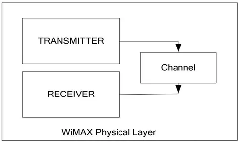
This paper discusses about the implementation and performance analysis of WiMAX system. The transmitter and receiver sections are designed with a Channel and implemented on FPGA module. The channel module models the noise that mixes with the transmitted signal and passes the noise added signal to the receiver. The implementation of the system is verified by transmitting a binary sequence of data through the transmitter sections, allowing the transmitted signal to enter the receiver and extracting back the binary sequence of data. The WiMAX system implemented here makes use of an additive White Noise module that is implemented in hardware to act as a source of noise to the signal.
a) Background
The WiMAX is a form of wireless transmission architecture which provides the speedy communication at low maintenance cost. This also gives the better use of bandwidth at higher frequency level. This part of the paper discusses the necessary concepts of the WiMAX system and its physical layer.
i. WiMAX system
The architecture of WiMAX system composed of various units in which base station (BS) and sink station (SS) are significant. Other components are CSN, MS, ASN, and CSN-GW, etc. The WiMAX Forum's Network Working Group (NWG) provides a network reference model according to the IEEE 802.16e-200. The reference model is logically divided into three units [5].
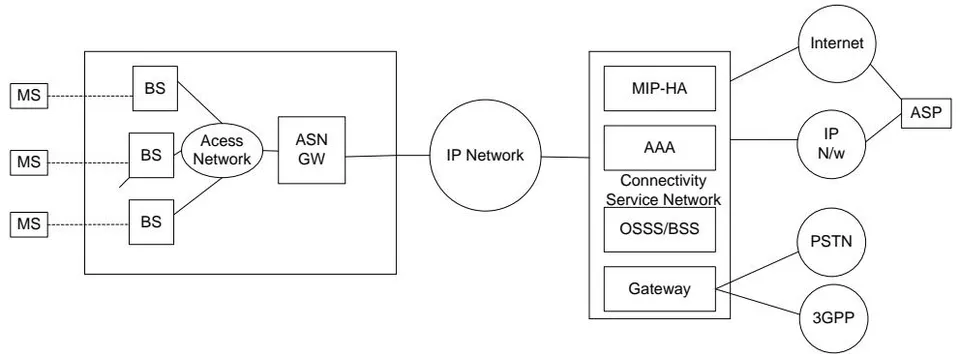
Mobile Station (MS): This acts as end-user equipment for accessing the mobile network. It is portable and provides data and voice communication facilities to the users.
Access Service Network (ASN): This is a network that provides access services with efficient scalability and high mobility. Its ASN-GW controls the network and coordinates among data and networking elements.
Service Network (CSN): Provides IP-connectivity, address and policy management, managing location between ASN, ensuring Quality of Service, roaming facility, and security.
ii. WiMAX Physical layer
This layer is mainly responsible for setting the connection among the communicating devices and transmission of the data bits. The physical layer design defines modulation type and transmission power requirements. WiMAX physical layer has two types of transmission techniques Time Division Duplex and
Frequency Division Duplex with operating frequency band below 11 GHz. The physical layer of IEEE 802.16 standard is based on OFDM which is mainly required for multimedia communication and digital video services as it provides very fast data speed on non-line of sight channels and multipath environment. The role of the PHY layer is to encode the MAC frames into analog signals and receive these signals from a communication channel [7].
b) Research Problem
The implementation of the physical layer of WiMAX system poses big challenges as this is a complicated standard and high-speed processing requirement. There are very few works that focussed on implementing the WiMAX physical layer on FPGA system, but design constraints could not satisfy for the real-time hardware implementation of the system. Here an effort is made to realize a Physical layer of WiMAX on
FPGA system with an improved throughput and FPGA design parameters.
II. LITERATURE REVIEW
This unit gives the discussion of the various research works towards the design and implementation of WiMAX based OFDM transmission system. Moises Sera [5] presented OFDM transmitter design as a part of Hiperlan/2 based transmitters. The issues in the implementation of OFDM based WLAN standard was presented by Ma.Jose Canet [6]. His work focussed on providing solutions to Baseband and IF OFDM signal generation. The work also benchmarked Optimised area results against system Generator results. Chris Dick[7] emphasized on designing the Software Defined Radio system on FPGA rather than on ASIC as FPGA provides a one-day solution to the implementation. His work provided a high-level view of FPGA implementation of OFDM receiver consisting of synchronization, packet detection; preamble correlates channel estimation and equalization functions. The implementation of 802.11 wireless standards on FPGA as a validating and prototype for ASIC was presented by Ludovico de Souza[8].Joaquin Garcia ad Cumplido [9] investigated the suitability of FPGA to support IF processing for 802.11a standard. The work majorly focussed on resource area and timing requirements that suit the implementation of rapid prototyping and also providing reconfiguration capability to support the different wireless standard. Awad et al. [10] implemented the physical layer of IEEE 802.20 and investigated the efficiency of OFDM transceiver. Lin [11] demonstrated the OFDM concept and investigated its efficiency changes by change in different parameters. The OFDM system was demonstrated by implementing the design in Matlab. Mohamed [12] presented an approach to implementing the OFDM system on FPGA. Harikrishna [13] presented FFT algorithm implementation on FPGA for WiMAX application. The author presented a memory based recursive FFT design which takes fewer gates, lower power and operates at high speeds. Upadhyaya et al. [14] presented an efficient FPGA implementation of address generation circuit for WiMax deinter lever. A QAM architecture for WiMAX application covering carrier synchronization and timing synchronization issues was presented by Sahoo et al. [15].
III. PROPOSED SYSTEM
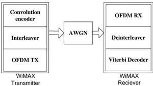
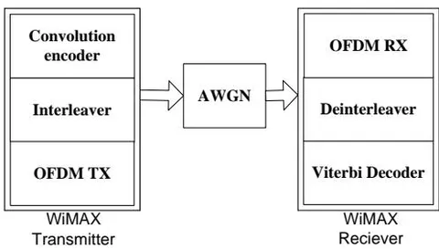
The OFDM physical layer system described here is an extension of the system described in chapter in chapter3 with few modifications that are added to the design. The modification to the hardware architecture of chapter1 includes the addition of Forwarding error correction technique. A convolution encoder for correcting the random errors and an inter leaver for overcoming the burst error effects are added at the transmitter section. The corresponding inverse function blocks such as a de-interleaved and a Viterbi decoder are added to the receiver section.
a) Convolution Encoder
This module comprises four inputs and two outputs. The global clock (_clk), reset (rst) and enable input signal act as control signals to the encoder. The Din signal serves as a single bit data input to the encoder. The convolution encoder developed is an encoder with a code rate of 1/3; hence the encoder output is a 3-bit code word (Dout). The encoder is also designed to give another output En_out which is high for the proper and valid working of the encoder. The En_out is also required for proper synchronization of the output code word. The convolution encoder is implemented considering a state machine implementation which comprises memory element and a combinational circuit. The state machine for the convolution encoder consists of M single bit shift registers and n modulo-2 adders (Ex-or gates). The shift registers are connected to the adders based on a generator polynomial. The number of adders in the state machine gives the length of code words generated.
b) Interleaver
This block reorders the coded symbols to counter the effects of burst errors on the transmitted coded symbols. The reordering of the coded symbols spreads out the burst errors rather than localizing it.
c) OFDM TX
The interleaved coded bits are transferred into Tx block for generating the OFDM signal. The OFDM TX block includes the following hardware modules 16 QAM, Symbol generation, zero padding, IFFT and Cyclic prefix(CP). The interleaved coded sequence is converted to one of the 16-QAM modulation symbols by passing the sequence through a QAM modulator. The QAM symbols are then zero padded and passed to a 256 point IFFT block. The cyclic prefix appends a 48-bit cyclic prefix code to generate a complete OFDM symbol of 304 bits. The OFDM signal will then be transferred over the channel via a Parallel to serial converter.

i. QAM
The coded data to be sent on the subcarriers are converted to QAM symbols using a 16-QAM module. The input4 bit data are mapped as one of the 16 QAM symbols. Each of the QAM symbols is represented as real and imaginary components after the mapping process. The input 4-bit data is transformed into 16 real parts and 16 imaginary parts.
ii. Symbol generation
This block constructs the OFDM symbol from the QAM symbols. In this block, the incoming QAM symbols are shifted four times to generate a single OFDM symbol. As the 16 bit Real and imaginary parts of each QAM symbol are shifted four times, the OFDM symbol constructed is of 64 bits. The incoming16-bit QAM symbols are grouped in four to create an OFDM symbol of 64-bit.
iii. Zero Padding
The 64 bit OFDM sample is zero padded in this block. The real-part and imaginary-part of the symbols generated from the SG block will be input to the Zero padding block to pad zeros. The zeros are padded to increase the sampling rate of the symbol. The 64-bit symbol data will be padded with extra 64 zeros to construct a 128 bit real and imaginary symbol data.
iv. IFFT
The extended real and imaginary symbol data are passed through an IFFT block to generate the OFDM symbol. The IFFT module developed is a 256 point IFFT.
v. Cyclic Prefix
The Cyclic prefix module extends the OFDM generate from the IFFT block to mitigate the ISI effects. It extends the symbol by prefixing the OFDM symbol by repeating the tail part of the symbol generated from IFFT. The cyclic prefix developed here extracts the last 32 bits from the IFFT generated OFDM symbol and prefixed it to the start of the symbol. Thereby a total of 288 bit OFDM symbol is generated.
d) AWGN Generator Module
The AWGN generator module is used as AWGN Channel Noise module in Fixed-WiMAX system. The AWGN generator module generates the white Gaussian noise (WGN) of SND (standard normal Distribution). There are so many digital-synthesizing techniques are available to generate the random Gaussian variables depends on the transformation of UDR (Uniform distributed randomly) Variables. The hardware architecture of AWGN generator module is designed by using different techniques [79] like Central limit theorem(CLT), Box-Muller(B-M) Method, Rejection-acceptance Methods, Wallace Method and ICDF(Inverse Cumulative Distribution Function). In our design, ICDF method is adopted.
e) OFDM RX
The OFDM signal received from the AWGN channel is passed through an RX block which consists of the following hardware modules; Inverse Cyclic Prefix, FFT, zero removal and QAM demodulator. The Inverse cyclic prefix removes the appended 48-bits of imaginary data and passes the 256 OFDM data to FFT block. The FFT block transforms the subcarriers to transform domain from which data is extracted by removing the zeros and demodulating. A 16-QAM demodulator maps the QAM symbols to code bits which will be forwarded to Inter leaver.
f) Deinterleaver
The deinterleaving operation is the reverse of interleaving. This operation is performed to rearrange the symbols that were interleaved in the transmitter section. The interleaving and deinterleaving operation are performed by reading and writing through memory buffers.
g) Viterbi Decoder
A Viterbi decoder is used at the receiver to decode the convolution codes. This decoder uses a Viterbi algorithm which uses trellis structure for decoding operation. The decoding of the convolution encoded sequence is performed by finding optimal path in the trellis structure for the received sequence. After obtaining the optimal path, a distance measure is used to receive and coded sequence to perform decision decoding.
IV. RESULTS ANALYSIS
This section the performance of the model designed is evaluated under two conditions of the channel 1) with fading and 2) without fading.
a) Simulation Outcomes
The BER performance of the WiMAX system for these two systems is analyzed for the above mentioned two conditions and compared with the theoretically generated BER values for the designed system. The theoretical values are obtained using BER calculation module present in MATLAB software.
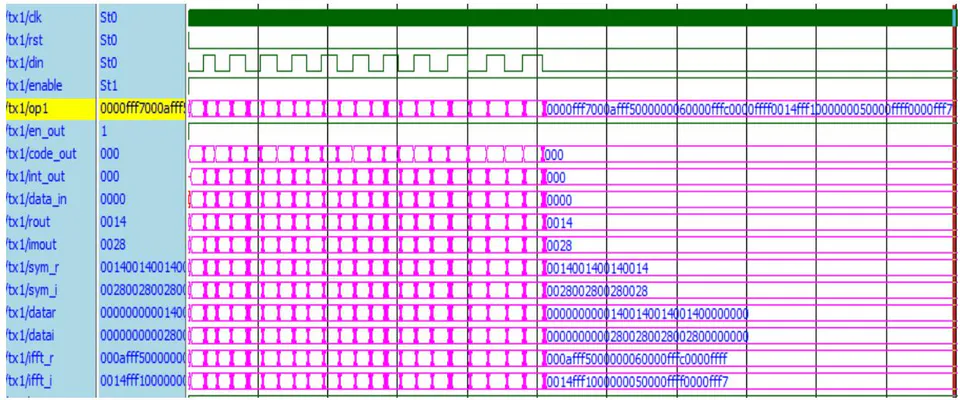
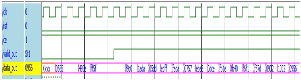
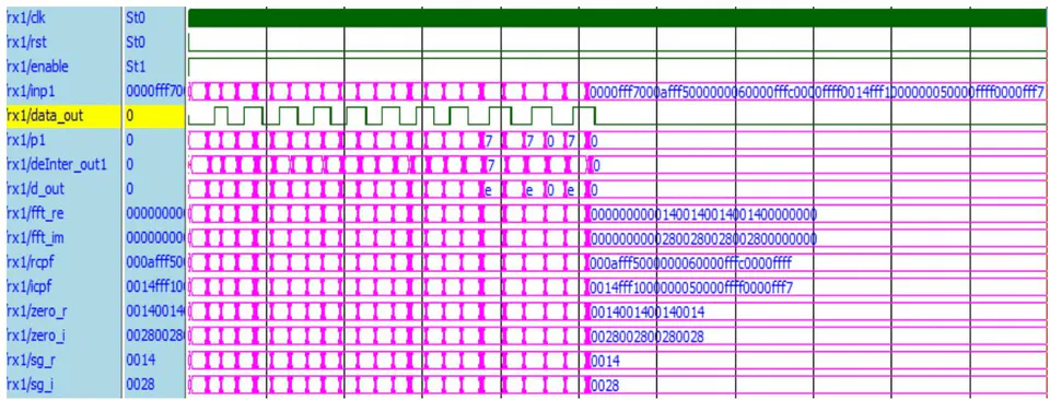
The AWGN Generator simulation results are shown in the figure 5.44. When clock is activated, initial reset has high, then low. The enable sign is set high.
Based on the design modules like T-URNG and I-CDF module designs. The random 16-bit is generated.
b) Performance Analysis
i. WiMAX System
The total number of clock cycles to process each input bits information, the proposed design takes 2485 clock cycles it can also call it as Latency. The FPGA Operating frequency is set to 100MHZ and clock period is set to 10ns. To process the 1024 bit data, the throughput or bit rate is calculated as follows.
Throughput = [1/ (2485 * 10 ns)] * 1024 bits = 41.20 Mbps.
| Optimization Parameter | Device: Kintex-7 FPGA | ||
| work[16] | proposed | Improvements | |
| Latency (clock cycles) | 3607 | 2485 | 31.06% |
| Throughput (Mbps) | 28.3 | 41.2 | 31.31% |
The latency and throughput are improved both around concerning previous WiMAX architecture [16]. The Bitrate complexity is reduced.
Similarly, the WiMAX system is area overhead, and hardware complexity is important in real-time implementations. So the proposed design is compared with work [17] for area constraints.
| Area used in WiMAX Systems | Virtex-6 | Work [17] | Proposed | Area Improved | ||
| Logic Utilization | Available | Used | Utilization | Used | Utilizat ion | |
| Number of Slice Registers | 301,440 | 165,792 | 55% | 8422 | 2% | 94.92% |
| Number of Slice LUTs | 150,720 | 102,490 | 68% | 17516 | 11% | 82.90% |
In work [17], the design is used system generator to generate the VHDL Code; It consumes more area because the code is auto-generated by system. The proposed design is written in Verilog HDL, and both the designs are synthesized in Virtex-6 X240T-2FF784 FPGA for comparison purpose. The proposed design gives around improvement in area overhead concerning work [17] as shown in the table-5.2.
ii. WiMAX Receiver
The main part of the receiver is Viterbi decoder to decode the convolution encoded bits. The timing analysis of modified Viterbi decoder for WiMAX system related to work [18] on Vertex-6. The proposed design achieves the maximum operating frequency with improvement as shown in the table-5.3. So it will improve the overall bit rate.
| Viterbi Decoder Timing Comparison | ||
| Timing Analysis | Device -Virtex -6 FPGA | |
| Work[18] | Proposed | |
| Minimum period(ns) | 15.5 | 10.083 |
| Maximum Frequency(MHz) | 64.516 | 99.179 |
| Setup Time(ns) | 20.8 | 1.537 |
| Hold Time(ns) | 5.8 | 0.659 |
The proposed modified Viterbi Decoder is compared with work [19] [20] for area for power consumption comparison as shown in the table-4.
| Viterbi Decoder Area and Power Comparison | |||
| Parameters | Virtex2 -2000 | Zynq-7000 | Zynq-7000 |
| Work[19] | Work[20] | Proposed | |
| Total Power (mW) | NA | 106 | 100 |
| Slices | 3444 | NA | 1918 |
| LUT's | 6303 | 5614 | 3201 |
The proposed modified Viterbi Decoder improved the area with respect to work [19] with slices and LUT's improvements. Similarly, with work [20], LUT's improved and improved in total power reduction in proposed modified Viterbi Decoder.
The Proposed WiMAX system checks the BER Rate, The number of bits transferred 100 and the number of errors occurred during the processed time interval is 14. So the BER rate is 0.14. Intermes of percentage is . The original number of bits recovered is .
V. CONCLUSION
WiMAX is a wireless Broadband access technology that implements the Wireless MAN (IEEE 802.16) standard. A WiMax physical layer was designed such that it can be efficiently implemented on FPGA system withimproved throughput and reduced design parameters such as area and power. The system was designed with Forwarding error correction capability and also the design incorporated a channel model that generated AWGN signal. The performance of the system was analyzed by comparing it with other designs. The design presented in this paper proved to provide a better throughput than other designs. The BER rate is performed better out of 100 bits, errored bits are 14, and the Original bits recovered is . The BER Rate is 0.14.