The performance of chip is degraded because of the short-channel effect (SCE) as the metal oxide semiconductor field effect transistor (MOSFET) size scales down. Silicon on insulator (SOI) technology helps to reduce the short channel effects and permits a good solution to the miniaturization. The electrical characteristics of fully depleted SOI (FDSOI) and partially depleted SOI (PDSOI) n-channel MOSFET (N-MOSFET) are investigated as silicon film thickness is varied in this paper. Both transistors are compared in terms of electrical parameters which are the threshold voltage, subthreshold slope, on-state current, leakage current and drain induced barrier lowering (DIBL). Silvaco TCAD tools are used for simulating both PDSOI and FDSOI MOSFETs. FDSOI MOSFET is superior to PDSOI MOSFET based on found simulation results.
## I. INTRODUCTION
Today devices of minimized area, reduction in power and increased performance have a great demand in the industry of microelectronics. The feasible technique of semiconductor industry to enhance productivity and performances is scaling of device [1]. The size of MOSFET has continually been scaled down [2]. The submicron technologies have created electrical operational challenges such as threshold voltage (Vth), subthreshold slope and leakage current due to the shrinking of the devices dimensions in MOSFET. The industry is facing difficulty to fulfill the Moore's Law using bulk devices which cause threshold voltage to decrease and leakage current to increase as length of channel decreases because of short channel effect (SCE). Silicon on Insulator (SOI) is considered as a potential alternative over conventional bulk MOSFET due to decreased silicon geometries and simple fabrication process. Radiation hardness, improved switching speeds, reduced leakage currents, better isolation, elimination of latch up and decrease in the short channel effects are some of the advantages of the SOI devices [3]. It has the intrinsic benefit of reduced source and drain areas and reduction of junction capacitance which makes these devices a potential candidate for low power and voltage applications [4-6]. SOI has several benefits over other technological solution such as no latch up, lower threshold voltage and better sub threshold slope [7-8]. There are two types of SOI, which are partially depleted (PD) and fully depleted (FD) depending on the thickness of the silicon film on the insulator. Usually, the thickness of silicon film is between 100nm to 500 nm for PD SOI device. For fully-depleted SOI devices, the thickness of silicon film is about less than 100nm. Due to removal of the floating body effect, FDSOI provides better short channel behaviour compared to the PDSOI. Hui et al. investigated impact of silicon film thickness on leakage current and threshold voltage in PDSOI and FDSOI [9]. This paper presents investigation between partially depleted and fully depleted SOI devices in terms of electrical parameters which are threshold voltage, subthreshold slope, on-state current, leakage current and drain induced barrier lowering. TCAD Silvaco software was used for simulation study of SOI devices. Simulation results revealed that the electrical characteristics such as threshold voltage, subthreshold slope and leakage current of fully depleted SOI outperformed than that of partially depleted SOI devices. There is difference in turn on voltage in fully depleted SOI (FDSOI) MOSFET. The threshold voltage is stable in partially depleted SOI (PDSOI) device due to thicker silicon film layer.
## II. METHODOLOGY
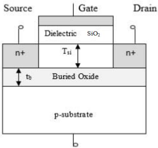
To study the electrical parameters on SOI MOSFET a schematic cross-sectional view of the SOI MOSFET, shown in figure 1, is simulated using Silvaco TCAD device simulator. The channel doping concentration is kept at $1 \times 10^{17} \mathrm{~cm}^{-3}$. The source/drain region doping concentration is kept at $1 \times 10^{20} \mathrm{~cm}^{-3}$. Gate length of the device is $1 \mu \mathrm{m}$. Gate oxide $(\mathrm{SiO}_2)$ thickness and buried oxide thickness are $18 \mathrm{~nm}$ and $0.4 \mu \mathrm{m}$ respectively. The total device length including drain, channel and source is $3 \mu \mathrm{m}$. Shockley-Read-Hall recombination, field-dependent mobility model and impact ionization model from Selberherr [10] was used for the simulation. Newton methods is used as numeric methods for simulation.
 Figure 1: Schematic view of SOI MOSFET
## III. RESULTS AND DISCUSSION
The n-channel PDSOI and FDSOI MOSFET has been investigated in terms of electrical parameters by simulation results obtained using Silvaco TCAD simulation software. Atlas syntax is used to create SOI structures and TonyPlot is used to display simulation results.
The impact of silicon film thickness on SOI MOSFET's electrical parameters are shown in table 1. FDSOI MOSFET has thickness of silicon film below $0.1\mu \mathrm{m}$ while for PDSOI it is greater than $0.15\mu \mathrm{m}$ for the simulated structure [11].
Table 1: The impact of silicon film thickness on electrical parameters of SOI n MOSFET
<table><tr><td>Silicon Film Thickness(μm)</td><td>Threshold Voltage,Vth(V)</td><td>Subthreshold slope(mV/dec)</td><td>On-state current,Ion(μA)</td><td>Leakage current,loff(pA)</td><td>DIBL(mV/V)</td></tr><tr><td>0.07</td><td>0.3206</td><td>65.45</td><td>81.89</td><td>12.42</td><td>74.84</td></tr><tr><td>0.09</td><td>0.4686</td><td>67.15</td><td>68.12</td><td>0.415723</td><td>113.34</td></tr><tr><td>0.11</td><td>0.6081</td><td>86.75</td><td>55.56</td><td>0.301249</td><td>166.66</td></tr><tr><td>0.13</td><td>0.6731</td><td>94.5</td><td>46.16</td><td>0.241121</td><td>178.18</td></tr><tr><td>0.15</td><td>0.6846</td><td>95.92</td><td>42.69</td><td>0.194797</td><td>180.73</td></tr><tr><td>0.20</td><td>0.6869</td><td>96.26</td><td>41.53</td><td>0.288933</td><td>179.56</td></tr><tr><td>0.25</td><td>0.6863</td><td>96.27</td><td>41.27</td><td>0.347851</td><td>177.83</td></tr><tr><td>0.30</td><td>0.6902</td><td>96.74</td><td>40.35</td><td>0.284068</td><td>175.69</td></tr></table>
The gate to source voltage needed to turn on the MOSFET is defined as threshold voltage, $V_{\mathrm{th}}$ [8]. Smaller threshold voltage satisfies high performance of device with technology scaling [12]. The threshold voltage for PDSOI is above 0.68 V and for FDSOI below 0.47 V as extracted from simulation results and also shown in figure 2. So the turn on voltage of PDSOI is larger than FDSOI from the results. This is the reason for FDSOI devices consuming less power and gaining higher speed.
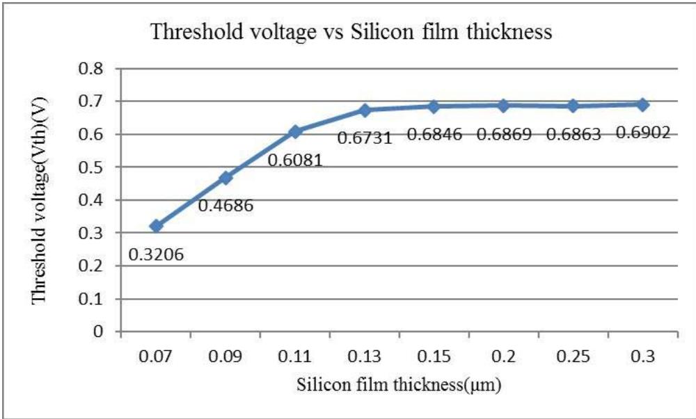 Figure 2: Threshold voltage versus silicon film thickness
A steeper subthreshold slope helps MOSFET to gain fast switching [13]. As silicon film thickness decreases, the steeper subthreshold slope becomes as from figure 3 which strongly increases the device speed. Comparison of subthreshold slope between FDSOI and PDSOI n-MOSFET is shown in figure 4.
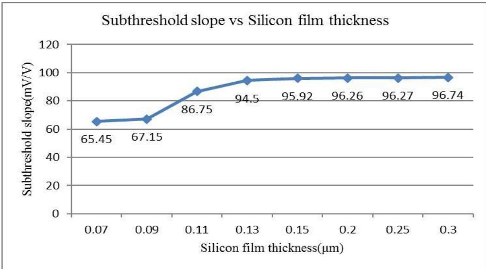 Figure 3: Subthreshold slope versus silicon film thickness
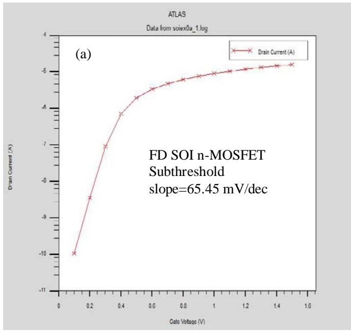
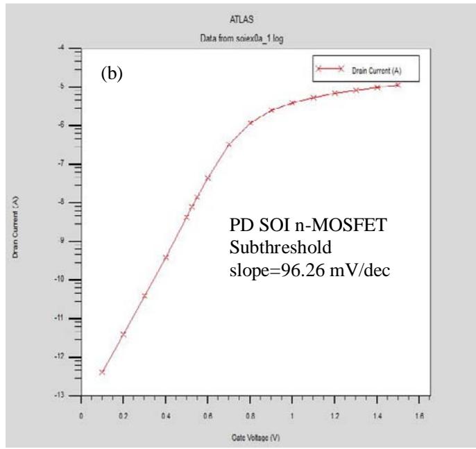 Figure 4: Comparison of subthreshold slope between (a) FDSOI and (b) PDSOI n-MOSFET
A high on-state current $(I_{\mathrm{on}})$ is needed to increase the driving force of the device. From figure 5, it can be said that the on-state current is greater when thickness of silicon film is reduced.
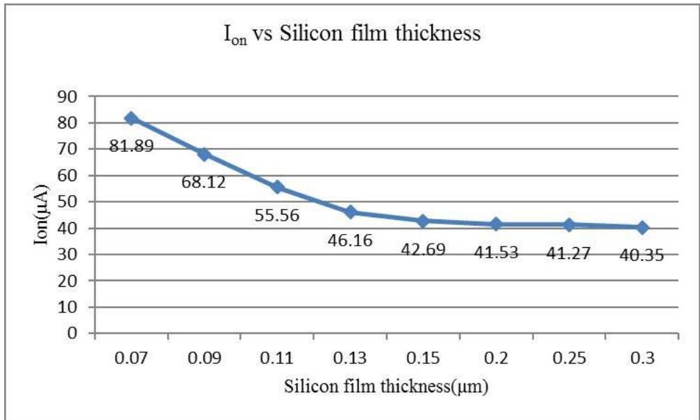 Figure 5: On-state current versus silicon film thickness
As threshold voltage is increased, the leakage current $(I_{\mathrm{off}})$ is decreased [14]. It can be decided that in PDSOI the leakage current is lesser but the variation is insignificant as shown in figure 6. Static power dissipation is created by leakage current when the device is not powered [15]. Static power dissipation will be small if leakage current is smaller. Thus, from the simulation results the static power dissipation of PDSOI will be smaller compared to FDSOI.
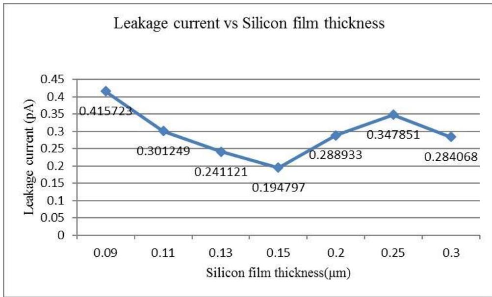 Figure 6: Leakage current versus silicon film thickness
Drain induced barrier lowering (DIBL) is an indication for short channel effects. Devices with smaller channel lengths and large bias on drain are vulnerable to DIBL effect. As thickness of silicon film increases from $0.07\mu \mathrm{m}$ upto $0.15\mu \mathrm{m}$, the DIBL value increases from $74.84\mathrm{mV} / \mathrm{V}$ to $180.83\mathrm{mV} / \mathrm{V}$ as shown in figure 7 which degrades short channel effects. As silicon film thickness increases from $0.15\mu \mathrm{m}$ to $0.3\mu \mathrm{m}$ DIBL value improves slightly. But it does not reach the same improved DIBL value compared with silicon film thicknesses between $0.07\mu \mathrm{m}$ to $0.1\mu \mathrm{m}$. Therefore SOI with silicon film thickness of $0.07\mu \mathrm{m}$ has the best DIBL parameter value which makes it less sensitive to short channel effects. Therefore, the impact of drain voltage on the device threshold voltage reduces.
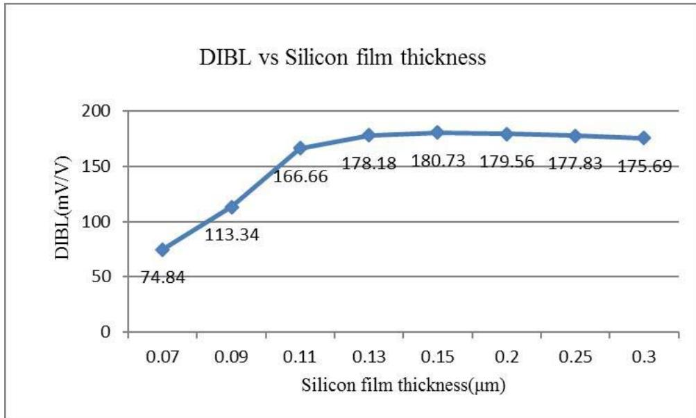 Figure 7: DIBL versus silicon film thickness
## IV. CONCLUSION
PDSOI and FDSOI has been compared in terms of electrical characteristics using Silvaco T-CAD Simulator. It is concluded that with increase of thickness of silicon film, the threshold voltage and subthreshold slope increased on SOI MOSFET which allows a smaller operating voltages and a higher switching speed for FDSOI. PDSOI can ensure a low static power dissipation as leakage current is small. But the leakage currents are in pA $(10^{-12})$ range for both SOIs. The DIBL parameter value shows that FDSOI is less sensitive to short channel effects. Based on the results obtained, FDSOI MOSFET displays superior performance compared to PDSOI MOSFET because of its lesser threshold voltage, steeper subthreshold slope, high on-state current and improved DIBL value in the device.
Conflict of Interest
The author declares that there is no conflict of interest.
Generating HTML Viewer...
References
15 Cites in Article
F Rahou,A Guen-Bouazza,M Rahou (2013). Electrical characteristics comparison between fully-depleted SOI MOSFET and partially-depleted SOI MOSFET using Silvaco software.
Yusnira Husaini,Mohd Ismail,Ahmad Zoolfakar,Norhazlin Khairudin (2010). Electrical characteristics comparison between partially-depleted SOI and n-MOS devices investigation using Silvaco.
James Kuo,Shih‐chia Lin (2001). Low‐Voltage SOI CMOS VLSI Devices and Circuits.
Y Taur (2001). Analytic solutions of charge and capacitance in symmetric and asymmetric double-gate MOSFETs.
Neeraj Gupta,Janak Patel,A Raghav (2015). A Study of Conventional and Junctionless MOSFET Using TCAD Simulations.
Sonam Rewari,Subhasis Haldar,Vandana Nath,S Deswal,R Gupta (2016). Numerical modeling of Subthreshold region of junctionless double surrounding gate MOSFET (JLDSG).
N Gupta,J Patel,A Raghav (2018). Performance and a new 2-D analytical modeling of a Dual-Halo Dual-Dielectric Triple-Material Surrounding-Gate-All-Around (DH-DD-TM-SGAA) MOSFET.
N Gupta,J Patel,A Raghav (2018). An Accurate 2D Analytical Model for Transconductance to Drain Current ratio (gm/Id) for a Dual Halo Dual Dielectric Triple Material Cylindrical Gate All Around MOSFET.
H Wei,S Ruslan (2019). Investigation of FDSOI and PDSOI MOSFET characteristics.
No ethics committee approval was required for this article type.
Data Availability
Not applicable for this article.
How to Cite This Article
Towhid Adnan Chowdhury. 2026. \u201cInvestigation the Impact of Silicon Film Thickness on FDSOI and PDSOI MOSFET Characteristics\u201d. Global Journal of Research in Engineering - F: Electrical & Electronic GJRE-F Volume 23 (GJRE Volume 23 Issue F2).
Explore published articles in an immersive Augmented Reality environment. Our platform converts research papers into interactive 3D books, allowing readers to view and interact with content using AR and VR compatible devices.
Your published article is automatically converted into a realistic 3D book. Flip through pages and read research papers in a more engaging and interactive format.
Our website is actively being updated, and changes may occur frequently. Please clear your browser cache if needed. For feedback or error reporting, please email [email protected]
Thank you for connecting with us. We will respond to you shortly.