

I. INTRODUCTION
First obtained and investigated characteristics of double-barrier structures created on the same plane. Shown advantages over conventional structures. First obtained and investigated characteristics of double-barrier structures created on the same plane. Shown advantages over conventional structures. With the introduction of the second barrier increases the integral sensitivity in photodiode ( ) times speed and 300 times in the structure. Non-ideality coefficient is small, due to the presence of an electrical field that is due to the drift mechanism in contact with the environment. UV radiation, for example, the case is being investigated jointly with the celebration structure. The influence of gamma radiation on the mechanism of current flow in the structure type Schottky barrier, and the p-n junctions. It is shown that the double-barrier structure can improve the photoelectric parameters of conventional detectors. Silicon photo detectors, still the most widespread type of photo converters. One of the main directions of increase of speed and increase in spectral sensitivity of modern receivers of radiation with one transition is creation of multi barrier structures. in which thanks to internal strengthening and growth of coefficient of collecting of the photo generated carriers - it is possible to improve significantly key parameters which meet the requirements and needs of optoelectronics. Reliability of work of the received structures under the raised conditions of radiation, as detectors of ionizing radiation is an actual task and makes a subject of our researches.
Recently for expansion of area of spectral sensitivity methods bringing to photocurrent growth in short-wave area of a range are widely used. Example can is – Verizon band structures; pulling fields, etc., based on reduction of speed of a superficial recombination. In our case such opportunity, but in planar execution it is possible to create at the expense of a field n-p-transition included in the opposite direction.
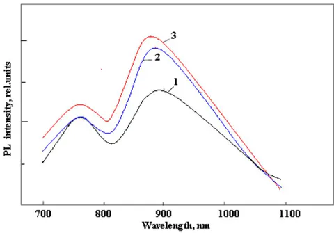
It is showing great interest in the study of photoluminescence features (PL) of short-wave radiation in the visible spectrum for efficiency c-Si-solar cells. Thus, the problem improves efficiency (c-Si) – photo elements consists of two parts: 1 - the re-emission of short-wavelength photons in the visible spectrum edge through the mechanism of direct optical transitions zone-zone silicon monohydrate, 2 - the effective conclusion of photo generated carriers across the spectrum of solar radiation. The forms of the spectra of these emissions, normalized to its maximum value each symmetrical with respect to the line:
where, - the frequency of the exciting radiation;
- frequency fluorescent light.
When excited photoluminescence monochromatic radiation is most likely the appearance of a low-frequency fluorescent light, although it is possible and the emergence of a high-frequency (anti-Stokes) radiation (Fig. 1). The spectra of the Stokes and anti-Stokes photoluminescence emissions. Spectral rules of photoluminescence due to the fact that the absorption of the exciting photon with energy.
where, h - Planck constant; - the frequency of the exciting radiation,
where, - fluorescent light frequency.
The energy difference spent on various processes in the material, in addition to photoluminescence. In cases where a photon energy of the exciting radiation is added to some of the energy of the thermal motion of the phosphor particles
where, a - coefficient depending on the nature of the phosphor;
k - is Boltzmann constant;
T - absolute temperature of the phosphor, there is anti-Stokes photoluminescence.
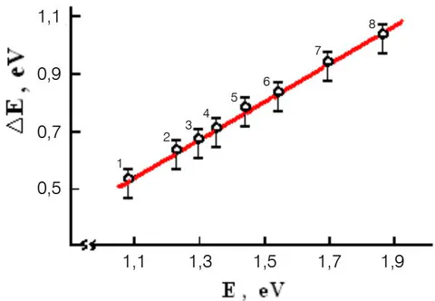
The optical properties of the structure dependence of hv makes it possible to determine the width of the band gap [4, 6] for the structure.
All of these structures of the optical absorption coefficient of the edge is described by the relation:
where, . - optical band gap for each film. B - coefficient of proportionality. The value is determined by extrapolation
Depending of hv for each sample. The quadratic dependence (2) obtained theoretically for Tauc model [7-9], which describes the density of states of the mobility gap.
II. CONCLUSIONS
Thus, it can be argued that the main role in the electrical losses studied silicon structures play oxygen centers (V2 + O and V + O). With increasing irradiation dose, and the annealing temperature increases, especially CVC and due to the change of spectral characteristics resistance n-Si (the base region of the structure) caused by the accumulation (increasing dose) and the disappearance or rearrangement (for annealing), radiation-induced defects. Known that the defect capture rate electrons and (or) the hole in the first place depends on the capture cross section and the position of the energy level in the forbidden band. These parameters are essentially the "individual" characteristic defect [6, 9]. Upon annealing, the structure is changing the point of radiation defects and their disappearance. In this case mainly the accumulation of similar defects. Comparison with literature data shows that the main role in the photovoltaic losses of these structures play an oxygen centers (V2 + O and V + O). With further increase of radiation dose an irreversible reduction of photosensitivity due to a significant increase in the resistance base.