I. INTRODUCTION
As the world is developing day by day the energy consumption is also increasing. We need much electricity than before but our sources are limited. Fossil fuel is limited and decreasing. Besides Fossil fuel based conventional power generation system emits a large number of greenhouse gases (CFC) which creates contamination of the environment. Sources of renewable energy can be the substitute remedy to generate power. Sun is where all energy comes from resources. Solar panel technology is one of the greatest technology in renewable energy technology.
Various kinds of solar cells are employed to produce energy. Some of them are, silicon solar cell with crystals, Amorphous Silicon Photovoltaic, Cd-Te photovoltaic cell, CIGS Photovoltaic cell, Multi-junction Photovoltaic cell, Tandem Photovoltaic cell, Perovskite Solar Cell etc. Perovskite Solar Cell is one of the largest technologies in the world. Many researchers are doing their research to raise the efficiency of this Photovoltaic cell.
II. LITERATURE REVIEW
Solar cell technology can be categorized into three generations. The initial cohort photovoltaic cells are wafer-oriented for example crystalline silicon photovoltaic cell. The solar cells of the second generation are organic solar cells that are based on thin films and belong to the third generation [1]. Perovskite solar cells are very efficient for future solar cell technology. Perovskite material can be efficiently used in solar cell, supercapacitor etc. The Perovskite solar cells have an efficiency of greater than . [2], [3]. No other kind of photovoltaic device has shown the startling rate of device efficiency growth in the past. Though the efficiency is increasing, it is quite challenging to achieve this efficiency in large scale industrial applications. The durability of this technology over the long term continues to be a concern [4].
Perovskite solar cell technology can be constructed using both organic based solar cell and Inorganic based solar cell. Organic - inorganic hybrid perovskite material is showing better efficiency than the inorganic perovskite material is recent researchers. Research efforts in hybrid organic-inorganic perovskites have intensified significantly. This emerging solar cell technology has shown rapid progress, with frequent advancements in power conversion efficiency percentages [5]. Notably, a study conducted in 2009 focused on a cell utilizing , demonstrating a high photo-voltage of and an efficiency value of [6].
Two years later, in 2011, a perovskite cell with nanocrystals sized at 2-3 nm achieved a solar electric efficiency of [7]. By the year 2023, significant progress was observed, with energy conversion efficiencies reaching an impressive [8]. In that same year, optimizing the treatment conditions for the layer resulted in a Power Conversion Efficiency (PCE) of [9],[10]. After nearly five years of dedicated research, the efficiency surpassed [3]. In recent research, the PCE of perovskite Solar cells are employing a variety of materials in an expanding manner and advanced technology.
III. METHODOLOGY
We employ utilizing numerical simulation with SCAPS-1D aims to improve the efficiency of a lead-free planar heterostructure perovskite solar cell with an n-i-p configuration. The device comprises an intrinsic layer made of methyl ammonium tin iodide (MASnI3) serving as both the i-layer and p-layer, while Spiro-OMeTAD is used for the p-layer. The n-layer is composed of SnO2. The goal is to optimize the design and parameters through simulation, enhancing the overall performance of the solar cell. [11].
A software program called SCAPS is used to simulate the electrical and optical characteristics of solar cells. It's frequently used to evaluate and improve many kinds of solar cell devices, such as silicon, organic material, and perovskites-based ones. [13]
There are multiple steps in the SCAPS simulation, and the particular techniques used can change depending on the kind of solar cell under study. Here's a broad rundown.
a) Numerical Modeling
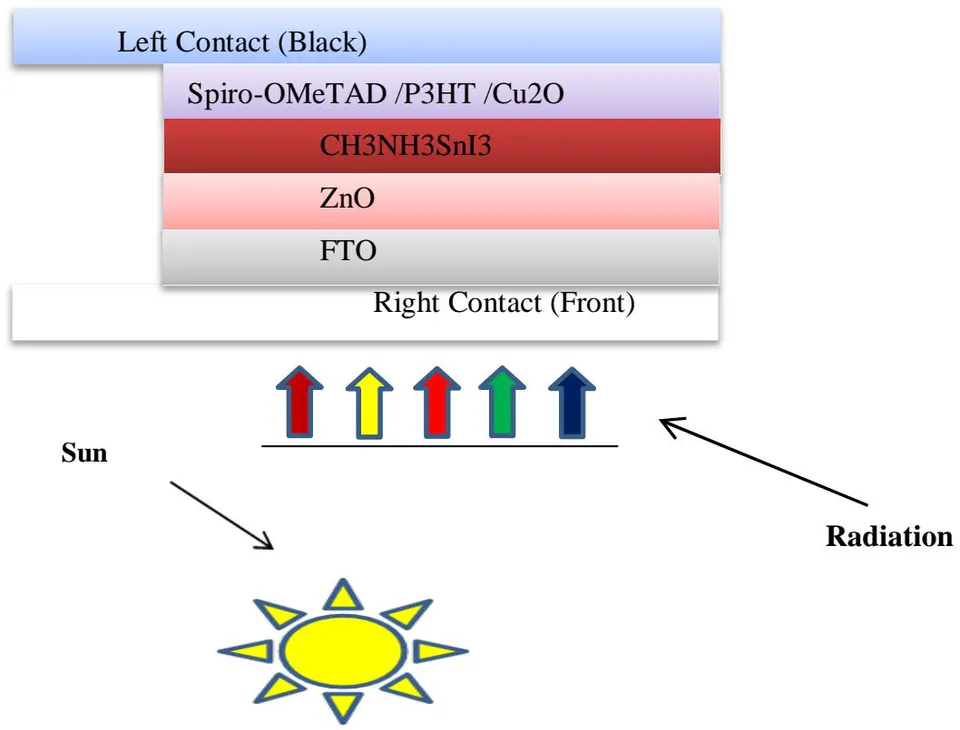
The design is a standard CH3NH3SnI3, based on PV cell structure. Figure 1, shows the cell is composed of an absorber layer, an n-type (ZnO), which represents an ETL layer, placed at the bottom, and the top of the p-type (Spiro-OMeTAD/P3HT/Cu2O), which represents an HTL layer. [12]
b) Parameters
Thickness, band-gap energy, electron affinities, effective density, effective VB density, effective density, electron mobility, hole mobility, effective density, donor concentration, and acceptor concentration are among the electrical properties. It is possible to alter these electrical characteristics. The following tables provide information on the electrical parameters in the SCAPS1-D program. [14]
| Parameters | FTO [15] | ZnO [16] | CH3NH3SnI3 [17] | Cu2O [18] | Spiro-OMeTAD[19] | P3HT[20] |
| Thickness/nm | 400 | 100 | 1.700 | 200 | 200 | 200 |
| Band-Gap Energy Ea/ev | 3.5 | 3.300 | 1.3 | 2.170 | 3.170 | 1.7 |
| Electron affinity/ev | 4 | 4 | 4.17 | 3.200 | 2.050 | 3.5 |
| Relative permittivity er | 9 | 9 | 10 | 10.000 | 3.000 | 3 |
| Effective-CB density Nc/cm-3 | 2.2E+18 | 2.0E+18 | 1.000E+18 | 2.50E+20 | 2.200E+18 | 2.00E+21 |
| Effective-VB density Nv/cm-3 | 1.8E+19 | 1.8E+19 | 1.000E+19 | 2.50E+20 | 1.800E+19 | 2.00E+21 |
| Electron Mobility un/cm2/V.s | 2.00E+1 | 1.00E+2 | 1.600E+0 | 2.000E+2 | 2.000E-4 | 1.800E-3 |
| Hole mobility un/cm2/V.s | 1.00E+1 | 2.50E+1 | 1.600E+0 | 8.600E+3 | 2.000E-4 | 1.860E-2 |
| Donar concentration Nd/cm-3 | 2.00E+19 | 1.00E+18 | 1.000E+0 | 0 | 0 | 0.000E+0 |
| Acceptor Concentration Na/cm-3 | 0.000E+0 | 0.000E+0 | 1.000E+17 | 1.00E+19 | 12.000E+19 | 1.00E+18 |
Interface layer properties, SCAPS-1D allows users to run simulations to analyze how these properties affect device performance metrics like efficiency, open-circuit voltage, short-circuit current, and fill factor.
| Characteristics | HTL/Absorber | Absorber/ETL |
| Defect type | Neutral | Neutral |
| Capture cross section electrons (cm2) | 1.00E-19 | 1.00E-19 |
| Capture cross section holes (cm2) | 1.00E-19 | 1.00E-19 |
| Energetic distribution | Gaussian | Gaussian |
| Reference for defect energy level Et | Above the highest EV | Above the highest EV |
| Energy with respect to reference (Ev) | 0.6 | 0.6 |
| Total density (integrated Over all energies) (1/cm^2) | 1.00E+10 | 1.00E+10 |
IV. RESULT ANALYSIS
a) Impact of the Perovskite Absorbing Layer Thickness
The implementation of device's performance is significantly influenced by the absorber layer. The previously published data reveals that the photovoltaic parameters such as Jsc, Voc, The thickness of the absorber layer affects FF and PCE [22]. The thickness of the absorber layer was changed from to in order to obtain its portion in the device simulation. Figure 1 illustrates how the absorber layer's thickness influences the variation of photovoltaic parameters. For FTO/ZnO/CH3NH3Snl3/Cu2O/Au, it has been found that Voc drops as absorber layer thickness increases.


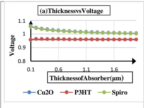
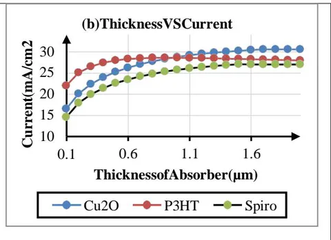
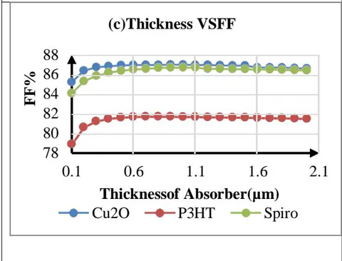
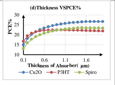
stays constant for the FTO/ZnO/CH NH Sn /P HT/Au configuration, while it changes for the FTO/ZnO/CH NH Sn /Spiro-OMeTAD/Au configuration. For all devices, the current from a short circuit rises as the degree of thickness of the absorber grows. The three devices' fill factor rises to before becoming saturated. For the FTO/ZnO/CH NH Sn /Cu O/Au Configuration, the maximum PCE is found to be when the absorber layer thickness is , VOC = 1V, Jsc = 31mA/cm2, and FF = . Diffusion length of the absorber layer is limited, which explains why PCE decreased with adjusted thickness.
b) Effect of the Thickness Variation HTL Layer
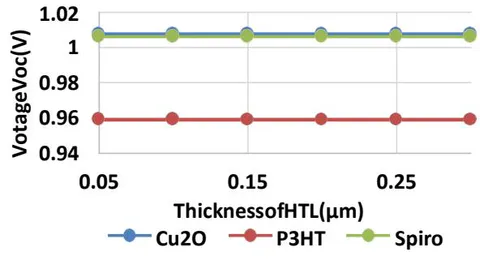
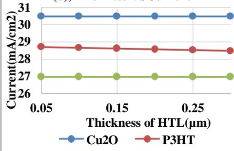
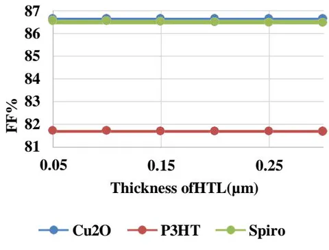
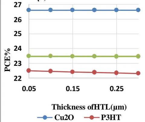
The demonstration of a perovskite SC is also significantly impacted by the thickness of its Hole Transport (HTL) Layer. The performance of the solar cell is determined by varying the thickness of HTL between 50 and . Voc, FF, Jsc, and PCE are seen to stay constant as HTL thickness increases.
c) Impact of the ETL Layer's Thickness Variation
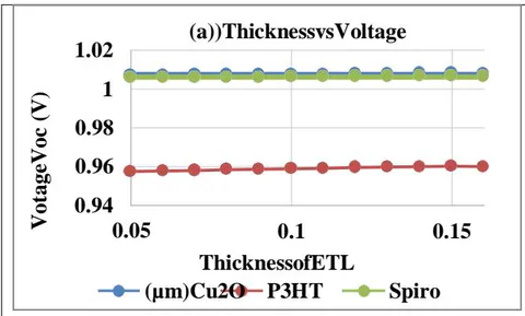
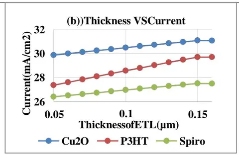
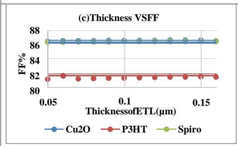
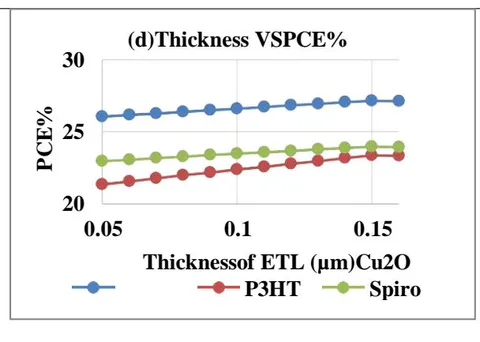
The breadth of the Electron Transport Layer (ETL) of the perovskite solar cell based can have a substantial impact on the functionality of the gadget. In this system, modification in ETL thickness can impact the perovskite solar cell. The ideal ETL thickness was determined in this study by varying the breadth of ETL between.05 μm and.15 μm. [24] It is observed that the ETL's thickness affects the solar cell's PCE and short-circuit current ( ), but not its voltage or flux (FF). With an increase in ETL thickness, Jsc and PCE both rise to 100 nm before becoming saturated. ETL is tailored to have a thickness of 100 nm.
d) Impact of the Absorber Layer's Accept or Density
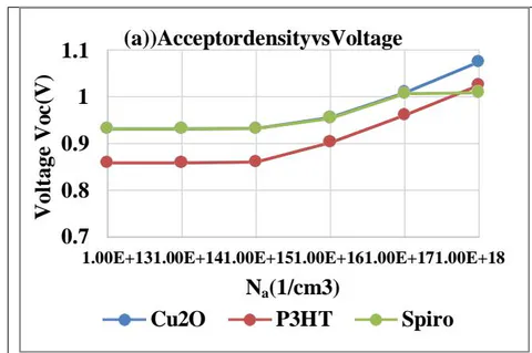
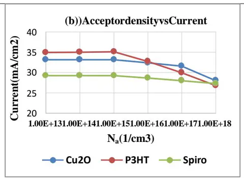
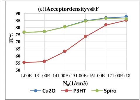
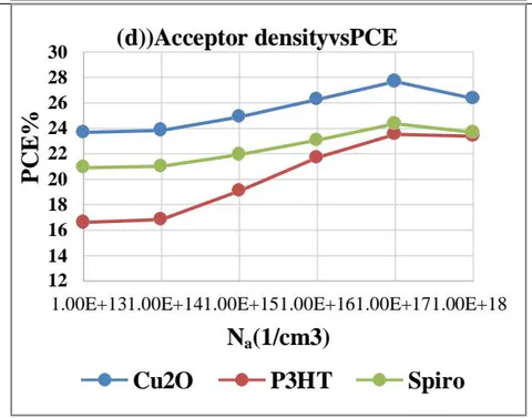
Amount of doping present in the exploiter has a significant impact on photovoltaic efficiency. The response of the suggested PSC for various HTLs with variable doping densities in exploiter layer is examined in this numerical analysis. Figure 4 (a) displays the , , , and efficiency of the planned PSC depending on the doping of the absorber concentration. The absorber layer's doping density has been adjusted between and . Up until , Voc and Jsc were nearly constant; after that, Voc increased and Jsc decreased for all configurations. Furthermore, fill factor increases as absorber layer doping concentration rises. On the other hand, PCE rises to before falling. After a given amount of doping, PCE decreases because it either produces additional defects or traps places where recombination might occur [25]. For all configurations, the absorber layer's ideal concentration of doping is .
e) Impact of Absorber Layer Defect Density
Figure 5 depicts the fluctuation of PV characteristics in conjunction with the defect density . To achieve optimal efficiency, it is crucial to comprehend how defect densities affect device performance, as recombination and generation take place within the layer designed for absorption. The primary cause of flaws an impacted device performance is a decrease in the quality of doping levels and the technique of doping within the absorber layer. Because, perovskite layer has many different defect energy levels, the Gaussian distribution provides an ideal way to explain the absorber layer's fault densities. The relevant Gaussian distribution equations of the acceptor and donor states are as follows:
- g DE = GMd exp [2 Ad2/(E-Epkd)2]
- gAE is equal to GMa exp [(E-Epka)2/2 Ad2]
Where GMd and GMa are the real flaws densities, Ad and Ea are the typical energy deviations of the acceptor and Gaussian levels, g1D € = G1 Md exp [[26]].
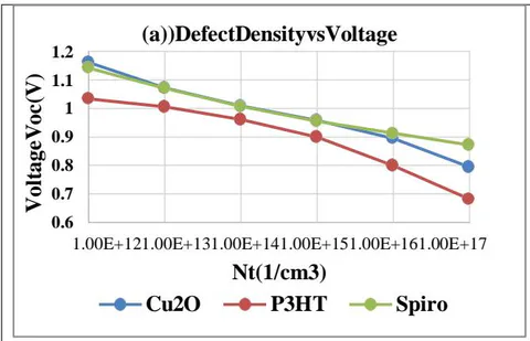
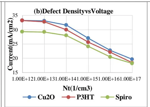
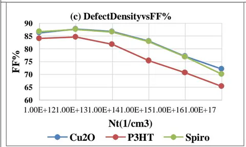
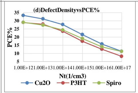
The acceptor location of peak energy is obtained positively from Ev and the donor Position of peak energy is measured. positively from , resulting in EPKD and Epka. Low quality perovskite layers, as shown by the plots, have a significant amount of defects densities, an elevated recombination rate of Tin , a decrease in the charge carriers' diffusion length, and eventually a decrease in the carriers' life duration. Above all, features have a big impact on how well the gadget performs. By altering the density of defects originating from to , we were able to compute the PV parameters. For , Spiro-OMeTAD, and P3HT, the corresponding efficiency values are , , and if the defect density is higher than . The model predicts that there will be a minimum of flaws in the absorber layer.
f) Band Diagram
Understanding the QE of a perovskite PV based on requires an understanding of its band diagram. The band diagram shows how e- and h+ flow throughout the solar cell as well as the various materials' energy levels. The band diagram for the FTO/ZnO/ combination is displayed in Figure 6. Light will first hit the TCO, then travel through the ETL and land on the absorber layer [27]. Since ETL has a bandgap of , it can absorb more sunlight. Electrons excited by photons having energies above the absorber layer's band gap, will move from the HOMO to the LUMO, leaving holes on the HOMO. Excitons or e-h pairs will result from this. The layer separating the absorber from the ETL will separate excitons. The openings will go to HTL. The charge carriers will be transported to the external circuit by two electrodes.
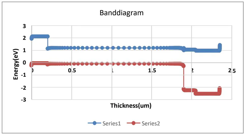
The band diagram illustrates the valence band and conduction band's energy levels for each material in the solar cell. It displays the perovskite layer's energy levels in the instance of . For effective charge separation and collection, these energy levels must line up. Charge Generation: Electron-hole pairs, or excitons, are produced when photons are absorbed by the perovskite layer. The separation of these excitons may be seen in the band diagram, where holes stay in the VB and electrons migrate to the CB.
Carrier Transport: The band diagram shows the energy barriers and routes that electrons and holes take to move across the various layers of the solar cell. This makes it easier to understand how efficiently carriers, like as and , can get to the electrodes to produce the current.
g) Quantum Efficiency
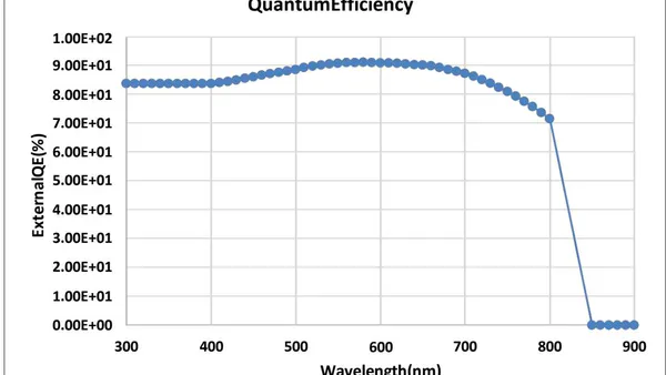
The ability of a solar cell, especially perovskite solar cells, to convert incident photons into electrical current is measured by its QE. It is frequently written according to wavelength, showing the cell's effectiveness at various light wavelengths [28]. The QE spectrum sheds light on the performance of the solar cell throughout the solar spectrum.
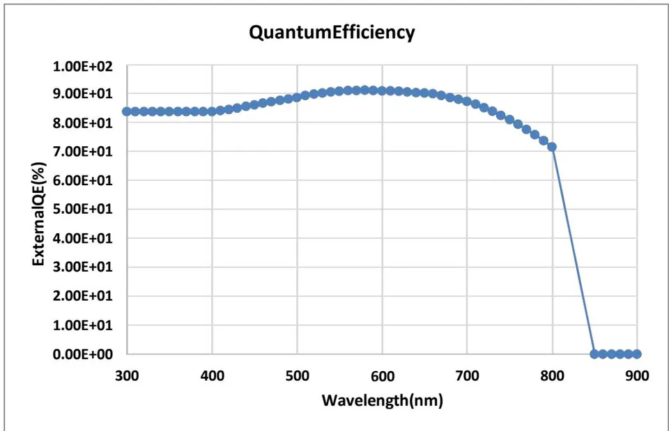
In the context of solar cells, quantum efficiency (QE) is the proportion of incoming photons overall to charge carrier number (electrons or holes) produced by absorbed photons. One kind of perovskite material used in solar cells is .
V. CONCLUSION
Using the SCAPS-1D software, a Sn-based perovskite solar cell was built and simulated for this work. Several HTLs were experimented with in this work to determine the ideal configuration. For , the highest efficiency was discovered. Furthermore, the absorber layer, HTL, and ETL thicknesses was adjusted to determine how the device's output changed. When the absorber layer's thicknesses, HTL, and ETL were.2 m,.15 m, and.17 m correspondingly, the highest efficiency was measured. Additionally, Doping concentration and defect density in the absorber layer were adjusted, and it was found that the maximum efficiency was attained at cm-3 doping concentrations and cm-3 defect densities, respectively. Maximum power conversion efficiency of 27.66% is displayed by the optimum configuration of FTL/ZnO/CH NH SnI /Cu O/Au, with , , and . The output of this lead-free organic inorganic Sn-formed PSC exhibits extremely encouraging findings, suggesting that the device can be manufactured in the future.