

I. INTRODUCTION
Single phase AC/DC rectifiers with a large electrolytic capacitor are commonly used for manufacturer and business issues. The main purpose to use diode rectifiers is to operate the switching power supply in data processing apparatus and to operate low power motor drive systems [1].
The large capacitor draws current in short pulses, which brings in a lot of problems including decreasing in the available power, increasing losses and reduction of the efficiency. In the conventional way of design, the capacitor voltage preserves the peak voltage of the input sine wave until the next peak comes along to recharge it .
The only way to recharge the capacitor is drawing the current from the input source at the peaks of the source waveform as a long pulse which includes an adequate amount of energy to nourish the load until the next peak. This is happens when the capacitor draws a large charge during short time, after the slowly discharge of the capacitor into the load. Therefore, the capacitor's current draws 5 to 10 times of the average current in or of the cycle period. Consequently, the source current has narrow and long pulses and the effective (r.m.s.) value increases [3], [4].
Customers with a large number of nonlinear loads also have large neutral current rich in third harmonics current. In order to increase the PF, decrease the losses and save the energy, then the input current harmonics (specially the third order harmonic) have to be eliminated. Several methods and techniques have been proposed to solve the problem of a poor power factor, which can be classified as active and passive methods .
Passive PFC circuits are generally simple, fewer components, smaller size and easy to design for small rating power (less than 200 watt). However, its bulky and not economical for large power ratings and the input power factor is (0.6 - 0.7) and THD = 150% in best conditions without using big size elements [6].
Active PFC circuits, can considerably diminish losses and costs associated with the generation and distribution of the electric power and significantly improved power quality. Therefore, APFC circuits are receiving more and more attention these days because of the widespread use of electrical appliances that draw non sinusoidal current from the electric power systems. However, PFC circuits require additional, more expensive and complex components . The author in , designed a novel PFC circuit that depends on the principle of limiting the work of the main capacitor in a manner which can eliminate the third order harmonic and improve the input PF into 0.99. However, this design has been used two Mosfets and high switching frequency equal to 200 KHZ which may increase the switching losses and reduce the efficiency.
In this paper, a new design of PFC converter has been introduced and presented in figure (1). The new design is depending on the flexibility of the parameters' variation which produces low harmonics, high input PF and high efficiency.
The new proposed design, reduces the required number of components into one Mosfet switch with low switching frequency equal to 20 KHZ, and uses small value of inductor which is smaller more than 96% of the inductors used in conventional boost PFC circuits, because the new proposed design focuses on shifting the harmonics components to the high frequency region and consequently eliminating the third order harmonic current, therefore the cost, the weight and the size of the new circuit will be reduced hugely.
The description of the circuit, operation topology, control circuit and operation stages are all described in section (II). The details of system's parameters are described in section (III). The discussion of simulation results and assessment are presented in section (IV), followed by an overall conclusion in section (V).
II. OPERATION PRINCIPLES AND ANALYSIS OF THE NEW PROPOSED CIRCUIT
a) Circuit's Description
The schematic circuit of the new proposed PFC circuit is shown below in figure (1).
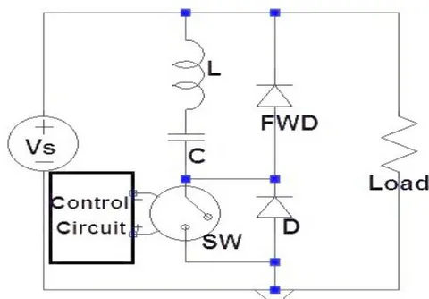
is the input DC source (represents AC single phase connected to full bridge rectifier), connected in parallel with LC resonant branch and MOSFET switch (SW) in parallel with the load. A control circuit has been designed in order to control the switching process.
b) Operation Topology
The new proposed circuit has the ability to control the working period of the capacitor. Consequently, the value of the input power factor, of the source current waveform and the value of the output ripple voltage can be controlled as well through using one switching devices.
The principle of this design is depending on the distributing of the working time intervals of the capacitor into two regions, at the beginning and at the end via using control circuit. This smart switching pattern would eliminates the third order harmonic component and improves the input PF as the third order harmonic is the most significant component in single phase systems.
This design uses a minimum number of components and minimum values of (L) & (C) a s capacitor turned off on the middle of each cycle, which shift the harmonics components to higher frequencies. consequently, reduces the size and the cost of the new proposed circuit.
This circuit is snubber-less circuit, because the freewheeling diode (FWD) presents an alternative path for the discharge current of inductor , so can the capacitor keep charged. Accordingly, (FWD) can avoid the negative part of and helps (C) to act as a snubber circuit in order to prevent the inductor's voltage ( ) to increase more than rated value of the source voltage, in this way (C) will protect the MOSFET switch from being burned in the effect of the high voltage spikes which may happen without the FWD.
c) Control circuit
A simple designed control circuit, as shown in figure (2) has been investigated in order to derive the MOSFET switch and control the switching frequency and duty cycle.
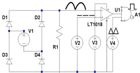
Briefly, the circuit consists of a dual input comparator which compares two signals (the first signal is the output of full wave rectifier and the second is a dc voltage source). The output of the comparator, which is a square wave, would be combine in a logic (And gate) circuit with a triangular waveform in 20 KHz frequency. the output of and gate will go directly to the gate of the MOSFET switch.
d) Operation stages
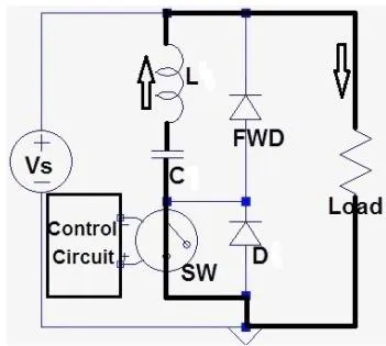
- First mode: This mode describes the time period , when the capacitor voltage . SW-ON/OFF, while is the moment when is equal or bigger than . The circuit shown in figure (3-a), illustrates the path of the current at this mode: In this period, (C & L) are discharging and feed the load.
because L, C and the load are series in this mode.
then the value of is approximately zero because the value of is very small (few micro henres).
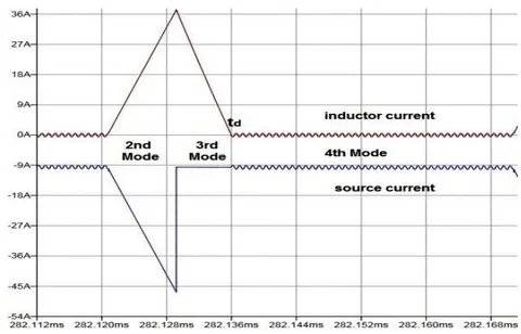
The full time period of the input source current waveform ( ) is shown in figure (4) with the details of nine time modes.
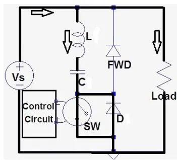
- Second mode: For the time period , when , and SW is ON. , is the moment when the pulses turns off. The circuit shown above in figure (3-b), the bold line illustrates the active path at this mode.
In this mode, the load, C & L are all connected to the source and charging with frequency pulses (20 KHz), as a result, high values and short time current spikes appear on the input current waveform because of the capacitor current.
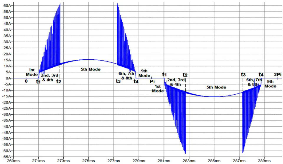
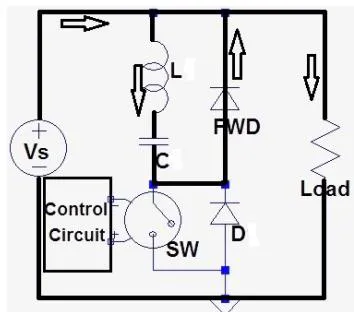
- Third mode: For the time period , when . This mode covers the interval time from switching OFF moment until ms. is the moment when or discharge to zero ampere for each pulse. The circuit is shown above in figure (3-c).
At this mode, (L) discharges its current to (C) until being zero (at the moment), while the inductor voltage is equal to and remains charged. This topology dose not require a snubber circuit as has been prevented.
is the resonance frequency.
At this mode, the load is fed by the source.
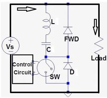
- Fourth mode: For the time period , when , SW is OFF (from until the next ON-pulse). The bold line in the circuit shown above in figure (3-d), clarifies the source current's path.
At this mode, the inductor current ( ) supposed to remain zero ampere. However, the internal capacitance of the diodes combines with stray inductance which form resonant circuit called parasitic resonant.
Due to this parasitic resonance, a sinusoidal current can flow into the inductor in a very high frequency (about 1.54 MHz) called self resonant (or parasitic) frequency ( ).
At the same time, follows waveform and oscillate around zero. & values are variable and change in accordance to the values of L, C, , and output load as it's clear from equations and shown in figures (4) and (5):
The capacitor voltage ( ) remains charged and considered as a constant value due to the value of which is approximately zero, then the value of is very small value.
is approximately 0.5 Amp. For ideal conditions, the internal capacitance of diodes is zero, therefore the parasitic resonance and can be considered as zero ampere.
Practically, a damper circuit (R=5Ω & C=1 nF) can be connected in parallel with the freewheeling diode in order to eliminate the resonance current (I0) totally, however, 0.1% of power losses can be increased in the circuit as a circuit of 3 kw output power, has only 3 watt losses in the damper circuit which is negligible. The modes (2,3,4) are repeating every ON/OFF switching pulse of SW.
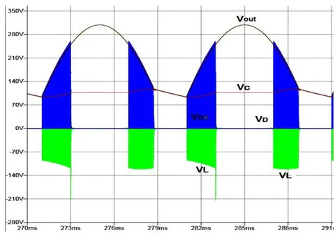
The figure (6), shows the full picture of , , waveforms. is in red color, is in brown color, is in green color, and is in blue color.
- Fifth mode: For the time period , when pulses are ON/OFF. is the moment when SW turns OFF. The circuit shown in figure (3-d), illustrates the active path of current at this mode:
Due to , therefore C and L are considered as disconnected (open circuit), because they are reverse biased when SW is OFF and (FWD) is reverse biased.
Therefore, C and L are neither charging nor discharging, then , but is a constant value.
Sixth mode: For the time period , when , SW is ON. is the moment when is greater than . The circuit is shown in figure (3-b). At this mode, C and L are charging and the load is fed by the source. All the derived equations in the 2nd mode are valid for this mode.
Seventh mode: For the time period , when . The circuit is shown in figure (3-c). At this mode, (C) is charging while is equal to until L fully discharges its current into zero ampere at the time of . All the derived equations in the 3rd mode are valid for this mode.
Eighth mode: For the time period , when , SW is OFF, for period until the next ON-pulse for . The circuit is shown in figure (3-d). still charged and slightly charging but approximately constant due to very small . remains charged and considered as a constant value due to the value of is approximately zero, then the value of dVC1 would be very small.
The modes (6,7,8) repeat themselves every ON/OFF switching of the MOSFET.
- Ninth mode: For the time period ms., when . SW-ON/OFF, the circuit is shown above in Fig. (3-a).
L & C are discharging while the R-load is fed by the main capacitor.
All the derived equations in the first mode are valid for this mode.
III. SYSTEM PARAMETERS
The proposed circuit has been simulated in LT-spice program and the parameters have been specified as the following table:
| Inductor (L) | ||
| Capacitor (C) | ESR = 0.035 Ω | ESL = 0 Ω |
| MOSFET | IPP070N8N3, N-channel | |
| Freewheeling diode | Schottky, (UPSC600) | |
| Parallel diode | Schottky, (MBR745) | |
| Load | Resistive | 20 Ω |
IV. SIMULATION RESULTS AND ASSESSMENT
An electrical circuit with , L = 20 H, C = 0.5 mF and MOSFET switch works in Khz controlled by a control circuit, has been designed and investigated by using Lt-spice simulink program.
R-load, inductor (L) and switching frequency of the MOSFET, are three main parameters in this circuit which could be changed in different values in order to find out the optimum design and parameters values in order to get low input , unity input PF, high efficiency, cheap, not bulky, small size and light converter.
Table (I), shows the relationship between different load values comparing it with fundamental input current , , , and input PF when L = 20 H and the switching frequency ( ) is 20 Khz.
| R(Ω) | (W) | (W) | η(%) | THD(%) | PF |
| 1 | 46354.5 | 44260 | 95.48 | 5 | 0.999 |
| 10 | 4920.2 | 4851.5 | 98.6 | 11.6 | 0.994 |
| 20 | 2506 | 2473 | 98.68 | 17 | 0.986 |
| 50 | 1038 | 1021 | 98.36 | 28.4 | 0.96 |
| 100 | 543.48 | 525 | 96.6 | 37 | 0.938 |
| 200 | 292.68 | 269.6 | 92.1 | 52.4 | 0.886 |
| 500 | 141 | 110.75 | 78.55 | 83.2 | 0.77 |
| 1000 | 90.2 | 56.1 | 62.2 | 111.7 | 0.667 |
Power factor has been calculated by using equation in [9], P.F =
The total input power, has been calculated via below equation [10]:
The maximum efficiency is 98.68% when input power is 2.5 kw when R-load = 20 Ω and (L) is 20 μH.
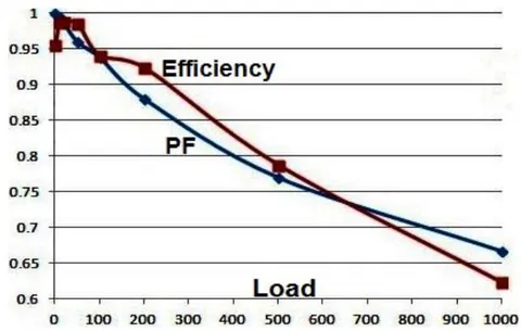
It can be concluded, from table (1) and figure (7) that the values of and input PF, inversely proportion with the increasing of the load value.
- Table (II) shows the relationship between different inductor values comparing with,, and input PF, when R-load = 20 Ω and= 20 kHz.
| L(uH) | (W) | (W) | (%) | THD(%) | PF |
| 1 | 2854.9 | 2679.4 | 93.86 | 55 | 0.876 |
| 10 | 2557.5 | 2510 | 98.1 | 24 | 0.972 |
| 20 | 2506 | 2473 | 98.68 | 17 | 0.986 |
| 50 | 2456 | 2434 | 99.1 | 10.5 | 0.994 |
| 100 | 2434.38 | 2415.5 | 99.2 | 7.2 | 0.997 |
| 200 | 2420.48 | 2403.7 | 99.3 | 4.9 | 0.999 |
| 500 | 2412 | 2395 | 99.3 | 3.5 | 0.999 |
| 1000 | 2407.3 | 2391.8 | 99.36 | 2.5 | 0.999 |
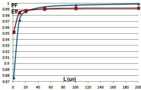
It can be concluded, from table (II) and figure (8) below, that the value of and PF, directly proportion with the increasing of inductor value.
- Table (III) shows the relationship between different switching frequencies of MOSFET comparing with , , and input PF when R-load = 20 and (L) is 20 H.
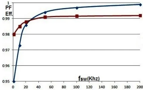
It can be concluded from table (III) and figure (9) that, the value of and PF directly proportion with the value of .
It can be concluded that, can be kept around (10 - 20) KHz in order to get approximately unity PF (0.98) at the input AC side when (L) is 20 H for 2.5 kw output power.
| (K) | (W) | (W) | (%) | THD(%) | PF |
| 5 | 2641 | 2574.8 | 97.5 | 33 | 0.95 |
| 10 | 2561 | 2515 | 98.2 | 23.8 | 0.973 |
| 20 | 2506 | 2473 | 98.68 | 17 | 0.986 |
| 50 | 2456.3 | 2434.2 | 99.1 | 10.6 | 0.994 |
| 100 | 2437.3 | 2415.8 | 99.1 | 7.6 | 0.997 |
| 200 | 2418.9 | 2405 | 99.4 | 5.6 | 0.998 |
| 500 | 2415 | 2397.2 | 99.2 | 3.9 | 0.999 |
| 1000 | 2414.8 | 2396.2 | 99.2 | 3.7 | 0.999 |
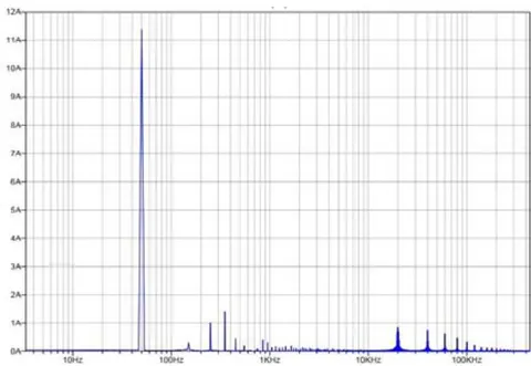
The figure 10, shows the Fast Fourier Transform (FFT) spectrum of the input source current. The total current harmonic distortion is , then the total input power factor is (0.986).
As it is shown in figure(10), the third order harmonic is not present at the input current waveform, and the only harmonic orders shown are the 5th and 7th order harmonics. This is because (C) was OFF at the middle of the waveformand the load was fed by the source.
In the case of the absence of freewheeling diode in the time intervals and (which represent the 2nd and 6th modes), the equation of inductor's voltage is:
(D) is the duty cycle of (SW) and because of the switching frequency ( ) is (20 KHz), therefore would be a very large value at this moment. Consequently, may be a reason for huge spikes on MOSFET's terminals and may burn the switch.
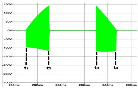
Generally, in this situation a snubber circuit would be proposed as a solution to suppress the high frequency spikes and to protect the MOSFET switch. However in this circuit, the main capacitor (C) would be act as a snubber circuit because of the existence of the freewheeling diode (FWD), which makes charges on the negative value of and prevent high voltage on the terminals of the MOSFET when its in open the status. As shown in figure (11), the inductor voltage does not increase more than 140 in spite of that the source voltage is 311 , because of the small value of (L).
- The required value of the inductance for the same voltage and power ratings in three level boost converter is (L), while the size would be doubled with the using of two inductors (2x2L) for the interleaved boost converter, on the other hand, the inductance would be doubled again (4L) for the conventional boost converter [11].
The inductor's value used in the literature in [12] for a (3 kw) output power using interleaved boost converter was , while the value of inductor (L) in the new proposed circuit is (20 H) for the same power ratings. This reduction of the inductor's value will effectively contribute in reducing the size, weight and the cost of the converter.
One of the significant features of this design, is that the inductor's current is not related to the value of source voltage (except in the 2nd and 6th mode) as usually happens in PFC circuits. This advantage can be utilized in order to reduce the value of (L) into few micro henrys and avoid high values. Consequently, can reduce the size, weight and the cost effectively.
Practically, the internal capacitor of the used diodes in the circuit would combine with the stray inductors and compose a parasitic resonant frequency . In order to get rid of the bad effects of , the rising time or the falling time can be changed, or alternatively a damper circuit can be added to the circuit or using clamping diodes and that's require additional components and complex design [13].
The inductor works like a proper choke or current limiter due to the high negative value of inductor voltage ( ) as its in counter direction of capacitor voltage ( ).
(L) charges in the time period because . On the other hand, for the time period , is zero because and are reverse biased. While, for the time period , (L) discharges as a positive current because . However, for time period of the next period, discharges as a negative current because and the R-load would be fed by which is the same capacitor's current ( ).
V. CONCLUSION
According to the simulation's results, the new proposed PFC circuit was able to reduce the to 17% with a unity power factor (0.986) at the input side and increases the efficiency to 98.68%.
The topology of reducing the conduction time of the main capacitor via dividing the waveform into three regions ONOFF-ON, can improve the efficiency, the input PF and reduce the at the input side.
In addition, preventing the capacitor (C) from work in the middle of the time period for about half of the time will eliminate the third order harmonic and shift the harmonics current to the high frequency region and that's will contribute in reducing the size of magnetics due to the small value of the inductor 20 H which produces a small amount of losses. Accordingly, the small inductor will effectively reduce the size and weight as used just one MOSFET, so the rectifier is not bulky any more, and thats reduces the cost of the converter.
Another advantage of this circuit is that the snubber circuit is not compulsory because of the presence of freewheeling diode. In addition, the design is considered as a high efficient design due to minimum number and small values of components and simple circuit design due to uses single switch.
The performance of this circuit has a wide range of flexibility because, the output ripple voltage, the input PF and can be improved via controlling the values of duty cycles of (SW), (L) and (C).
From graphical waveforms and tables of results analysis for different values of R-load, inductor (L), and switching frequency, can be concluded that the increasing of inductor value (L) and R-load values is required in order to get a constant unity power factor, small and high efficiency.
VI. ACKNOWLEDGMENT
The first author gratefully acknowledge the big support of the Higher Committee for Education Development (HCED) in Iraq.