It is of great practical significance to test and analyze the quality of silicon materials used in integrated devices and their changes in planar thermal process. This paper summarizes the international test, analysis and research results. The contents include polycrystal preparation, single crystal growth and its crystal defects, wafer cutting, grinding and polishing, wafer tracking observation and analysis in plane thermal process, generation control and elimination of induced dislocations, etc.
## I. INTRODUCTION
Nowadays, there is a very fashionable term "chip" and "chip engineering". Their essence is to prepare semiconductor devices on silicon wafers, such as diodes (P-N junctions, rectifiers), transistors (P-N-P or N-P-N), integrated circuits, including large-scale integrated circuits and super-large-scale integrated circuits. The so-called circuit is to integrate the diodes-transistors-resistors-capacitors with different parameters into a single circuit according to the purpose and needs of use, and then fabricate it on the silicon wafer by the method of planar process. The so-called "planar process" is produced by repeatedly arranging individual circuits into an array on a silicon wafer. Therefore, after the completion of the plane process for the production of integrated circuits, it is necessary to use an integrated device dicing machine to split out a single integrated circuit, that is, a silicon chip, and test each chip under a high-power magnifying glass, and then place the qualified silicon chip into an exquisite packaging box. After it is fixed, it is also connected, that is, to connect the output input point of the silicon chip with the input and output connector of the packaging box, and finally add the cover package to get the chip needed by the user. Please note that the pre-process and post-process of chip production are carried out in a highly clean purification room.
The planar process for the preparation of integrated circuits is quite complicated. the first step is to produce qualified silicon single crystals, including large-diameter and super-large diameter silicon single crystals, the purity of silicon single crystals, N-type/P-type impurity concentration, and crystal perfect have very strict requirements; the second is to cut the wafers with a certain orientation and thickness according to the requirements of different devices, and the wafers that can meet the requirements of the devices after strict grinding and polishing. The prepared wafer must also have a strictly required reference chip in order to arrange the chip pattern and ensure the yield of the final device.
After entering the thermal process, it becomes more complex, including oxidation-lithography, selective diffusion, epitaxy, re-oxidation-re-lithography, re-selective diffusion and so on. There is not only plane arrangement, but also the problem of multi-layer intersection. For example, the scale of lithography has now reached the nanometer and sub-nanometer scale, so the plane scale of selected diffusion also reaches the nanometer scale; there are also phosphorus (N-type) diffusion and boron (P-type) diffusion, as well as the concentration of diffusion doping. The cross-overlap between layers and the problem of diffusion depth and concentration distribution can form a P-N junction or P-N-P or N-P-N junction that meets the design requirements, as well as the parameters of resistance and capacitance, as well as the wiring of these diodes, transistors, resistors and capacitors, input and output wiring, and so on. For lithography, first apply photoresist, under the cover of the lithography mask, use the lithography machine to expose the selected area, etch the selected area, and remove the photoresist. It can be seen that lithography is very important in the chip plane process, in which the lithography machine is the most critical equipment. At present, there are ASML of the Netherlands, Nikon and Canon of Japan, and Shanghai Microelectronics of China.
 Fig. 1: Advertising map of an integrated circuit (or chip) after high magnification
An integrated circuit (or chip) after high magnification is shown in figure 1. Why it is used, what kind of integrated circuit to design, this is the task of the integrated circuit (chip) designer, how to use the plane process to produce qualified chips, this is the process designer of the plane process engineer and the art of the operators on the production line. What we are concerned with here is the problem of silicon materials in the process of silicon and its devices. The so-called material problems include the purification and ultrapurity analysis of polycrystals, the preparation of monocrystal silicon and crystal defects, and the preparation of silicon wafers (orientation of reference edges, directional cutting, grinding and polishing). As well as the generation control of crystal defects in the thermal process and the best thermal process and other material problems. We will discuss it in sections below.
## II. PREPARATION AND PURIFICATION OF POLYCRYSTAL SILICON
The preparation of polycrystal silicon is the use of the most common raw material quartz sand (also known as silica) on earth, which refers to silicon dioxide. Polysilicon is obtained by refining, and then a series of chemical and physical purification processes can be used to produce polysilicon with semiconductor purity. Some people say that the purity of electronic grade polysilicon can reach 11N, that is, 11-9s, that is $99.999999999\%$.
a) Smelting of quartz sand and purification of crude silicon [5] i. Smelting of quartz sand
Smelting uses charcoal or other carbon-containing substances such as coal and tar to reduce quartz sand to obtain silicon with a content of $98 - 99\%$, which becomes metallurgical grade silicon and crude silicon or ferrosilicon. The chemical reaction is
$$
\mathrm {S i O} _ {2} + 2 \mathrm {C} - > \mathrm {S i} + 2 \mathrm {C O}
$$
The main impurities in crude silicon are Fe, Al, C, B, P and Cu, which need to be further purified.
## ii. Purification of crude silicon
Silicon is insoluble in acid, so the preliminary purification of crude silicon is soaked with HCl, $\mathsf{H}_2\mathsf{SO}_4$, aqua regia, HF and other mixed acid to $99.7\%$ Si content. The chemical reaction formula is.
$$
\begin{array}{l} \mathrm {S i} + 3 \mathrm {H C l} - > \mathrm {S i H C l} _ {3} + \mathrm {H} _ {2} \\\mathrm {S i} + 2 \mathrm {C l} _ {2} - > \mathrm {S i C l} _ {4} \\\end{array}
$$
### b) Acquisition of ultra-pure polysilicon
The principle of further purification is to make use of the different boiling point of the substance and purify it by distillation in the distillation column. Because the boiling points of $\mathrm{SiHCl}_3$ and $\mathrm{SiCl}_4$ are $31.5^{\circ}\mathrm{C}$ and $57.6^{\circ}\mathrm{C}$ respectively, both $\mathrm{SiHCl}_3$ and $\mathrm{SiCl}_4$ are liquid at room temperature. High purity $\mathrm{SiHCl}_3$ or $\mathrm{SiCl}_4$ is obtained by distillation in a distillation column. Hydrogen is easy to purify and has very low solubility in Si, so the silicon obtained by reducing $\mathrm{SiHCl}_3$ and $\mathrm{SiCl}_4$ with $\mathsf{H}_{2}$ is semiconductor pure polysilicon. The decomposition reaction is as follows:
$$
\begin{array}{l} \mathrm {S i C l} _ {4} + 2 \mathrm {H} _ {2} - > \mathrm {S i} + 4 \mathrm {H C l} \\\mathrm {S i H C l} _ {3} + \mathrm {H} _ {2} - > \mathrm {S i} + 3 \mathrm {H C l} \\\end{array}
$$
The purity of the intermediate products obtained in each stage of purification can only be known by ultra-purity analysis, reaching several 9. For ultra-pure analysis, mass spectrometry, polarography and neutron activation are often used for statistical analysis. if trace or ultra-pure analysis is to be carried out, secondary ion mass spectrometry is a suitable method.
## III. PREPARATION AND TEST ANALYSIS OF SILICON SINGLE CRYSTAL
Up to now, silicon single crystals are mostly prepared by gas phase growth method, Czochralski method and floating zone growth method.
### a) Preparation of Silicon single Crystal
Silicon materials have been developed in two ways: one is to provide higher quality crystals (including the control and extraction of impurity distribution).
The second is to develop cheap silicon crystals of certain quality, which are mainly used to make silicon solar cells used on the ground, and the vapor phase silicon single crystals are simple in process, and the cost can be greatly reduced. The crystal quality meets the requirements of making solar cells.
Using chemical vapor deposition (CVD) method, using $\mathrm{SiHCl}_3$ or $\mathrm{SiCl}_4$ as raw materials, the silicon single crystal was reduced by $\mathsf{H}_{2}$, and the silicon single crystal was grown by vapor phase method using seed crystals with specified orientation (such as [110,111,112 and 115]) as silicon core, then grew freely in vapor phase $\mathrm{SiCl}_4 + \mathrm{H}_2$ environment and temperature $1150\sim 1160^{\circ}\mathrm{C}$, its length remained unchanged, while lateral free growth [2].
The Czochralski method is to heat the polysilicon through the thermal field, melt it into a melting state, control the liquid surface temperature at the critical point of crystallization by controlling the thermal field, and pull up from the liquid surface through the single crystal seed crystal above the liquid surface. with the rising of the seed crystal, the molten silicon grows into a cylindrical silicon single crystal according to the direction of the seed crystal.
Silicon single crystals are grown by this method with [111] and [100] orientations.
The floating zone method melts the polysilicon by local heating, moves the heating zone, and the melting part begins to crystallize. If the seed is placed at one end of the polysilicon material, the crystal will form a single crystal in the seed direction, and finally all the materials will be converted into single crystals. The principle is that the soluble impurities of raw materials are controlled or reformulated by generating a temperature gradient near the growth interface, so it has the function of purification.
The floating zone method is divided into horizontal zone melting method and suspension zone melting method. The growth process is as follows: (i) the crystalline material is made into an ingot in the crucible, the seed crystal is at the leftmost end of the crucible (horizontal zone melting method), and the seed crystal is at the top end of the suspension zone melting method; (ii) one end of the crucible is moved to the high temperature zone to form a melt; (iii) the crucible continues to move, the melt from the high temperature zone is formed, and the ingot entering the high temperature zone is melted; (iv) the other end of the crucible is moved out of the high temperature zone, and the growth ends.
b) Observation and analysis of the shape of silicon single crystals [6, 7, 8]
Figure 2 shows the cross-sectional views of vapor phase grown single crystals with three orientations of $< 111>$, $< 112>$ and $< 115>$.
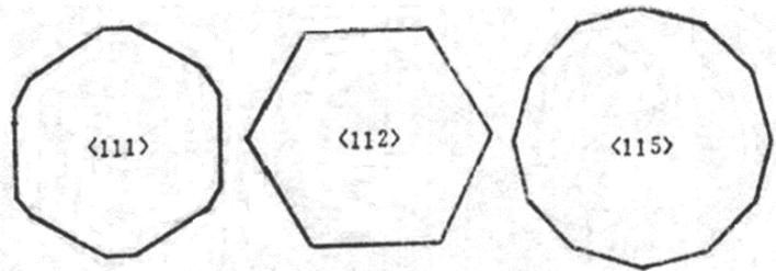 Fig. 2: Cross-sectional view of vapor phase single crystals with three orientations of $< 111>$, $< 112>$ and $< 115>$
The external shape of vapor grown silicon single crystal follows the principle that the total surface energy of all external surfaces is the minimum, and the normal growth rate of these planes is slower, and the surface energy is lower, which is generally a low index crystal plane [2]. The $< 111>$ oriented gas phase silicon single crystal is nearly hexagonal, with six $\{11\overline{2}\}$ faces and six edges as narrow planes $\{\overline{1}10\}$, and the $< 115>$ orientation is twelve prisms and two $\{1\overline{1}0\}$ faces, Four $\{\overline{4}11\}$ faces, four $\{\overline{6}11\}$ faces, two $\{\overline{5}52\}$ faces, the four plane areas are not much different; the orientation is $< 112>$ there are four $\{\overline{3}11\}$ faces and two $\{\overline{1}11\}$ nearly hexagonal prisms [1]. From these analyses, it is concluded that the crystal plane with the fastest growth rate in the normal direction is easy to disappear, and the crystal plane with the slowest growth rate is the slowest. From the point of view of the crystal structure, $< 110>$
with the highest linear atomic density grows the slowest, and it is the easiest to reveal. The $< 110>$ oriented gas phase silicon single crystal is almost tetragonal prism, and the surface is a pair of $\{100\}$ faces and $\{\overline{1} 10\}$ faces, which $\{\overline{1} 10\}$ is much wider than $\{100\}$. The $< 100>$ orientation should be square column, and all four cylinders are $\{110\}$.
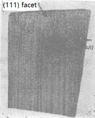
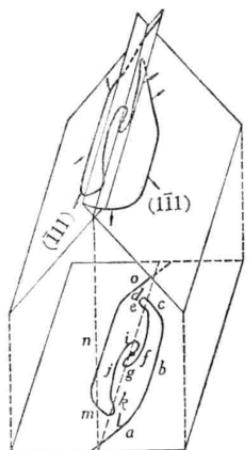
The silicon single crystal grown by Czochralski method and suspension zone melting method is cylindrical in shape. The surface of [111]-oriented single crystal shows three growth edges with cubic symmetrical distribution, and the surface of [100]-oriented single crystal shows four growth edges with four symmetrical distribution. Their orientation relations are given by polar diagram analysis and experimental observation [4]. This gives the fabrication orientation of the reference plane of the (111) and (100) wafers, that is, the reference plane of the cylindrical single crystal with $< 111>$ orientation should be parallel to the line between the two edges of the vertical cross section, and the reference edge of the (111) wafer is in the $< 110>$ direction. The reference plane of the $< 100>$ oriented cylindrical single crystal should be parallel to the diagonal of the four growth edges, so that the reference edge of the (100) wafer is also $< 110>$ direction. It is also pointed out that when making integrated circuits with (111) chips, the long side of the rectangular chip should be strictly parallel to the reference edge in the $< 110>$ direction when laying out the circuit graphics for the first time. It is also pointed out that when slicing with a dicing machine, the first knife should be parallel to the reference edge, and after the second knife perpendicular to the first knife is completed, the wafer should be rolled along the vertical direction of the reference edge, so as to ensure that the wafer breaks along the $\{111\}$ solution tilted to the wafer surface. For the fabrication of integrated circuits with $\{100\}$ oriented wafers, it is only required that either side of the rectangle or square should be parallel to the reference edge of the wafer when laying out the circuit for the first time. In this way, the best slicing yield of integrated circuits can be guaranteed, which is completely based on theory.
# IV. OBSERVATION OF SEVERAL PHENOMENA IN THE GROWTH OF DISLOCATION-FREE SILICON SINGLE CRYSTALS
Although some devices require uniform distribution of low-dislocation wafers, dislocation-free silicon single crystals are still the most widely used materials. It is of practical significance to study and summarize the problems in the growth of dislocation-free silicon single crystals.
a) Generation, extension and elimination of weld surface defects
Dislocation-free silicon single crystals grown by Czochralski method, zone melting method or pedestal method should be induced by single crystal seeds with a certain crystal orientation. After baking, the directional growth of the new crystal begins when the seed crystal is in contact with the melt. The interface between the seed and the new crystal is called the fusion surface. The seed which is cold or hot to a few hundred degrees will instantly come into contact with the melt above $1420^{\circ}\mathrm{C}$, which will produce great thermal fluctuation and thermal stress, so a large number of dislocations will be introduced into the seed end of the fusion face. On the one hand, these dislocations will return to the seed, on the other hand, they will move and extend in the new crystal. From this point of view, it does not matter whether the seed crystals grow dislocation-free single crystals or not.
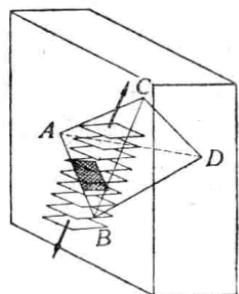
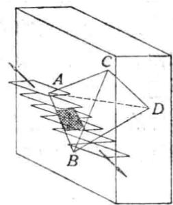
In order to prevent the dislocation produced by the weld surface from extending into the crystal, 1956, The necking-thinning technology proposed by Dash [6] is very effective. A simplified diagram of the motion and extension of the dislocation in the thin neck is shown in figure 3. The silicon crystal has a diamond cubic structure, and the dislocations mainly lie on the $\{111\}$ slip plane. The orientations of edge dislocations and screw dislocations are $< 112>$ and $< 110>$, respectively.
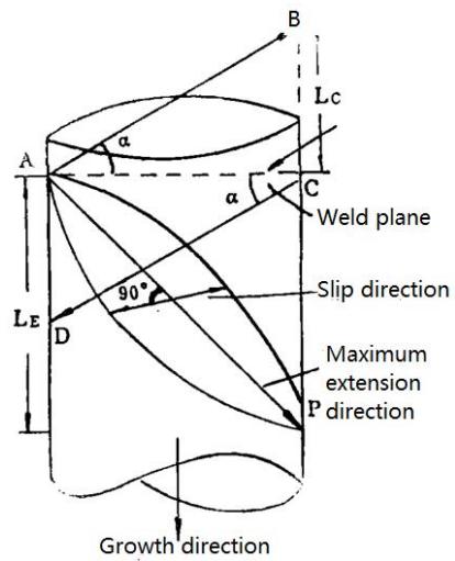 Fig. 3: Schematic diagram of the movement and extension of dislocations in a thin neck
The extension direction of the dislocation line is the direction of the dislocation line, the climbing direction of the edge dislocation is $<111>$, the slip direction is $<110>$, and the screw dislocation can slip on any crystal plane including the dislocation line and the Bell vector. We consider that the projection of the maximum climb, slip and extension distance of a dislocation on the $\{111\}$ plane at an angle to the growth axis is $L_{Cmax}$, $L_{Gmax}$ and $L_{Emax}$, respectively, which can be expressed as follows:
$$
\begin{array}{l} L _ {C m a x} = D t g \alpha \\L _ {G \max } = 0 \\L _ {E \max } = D c t g \alpha \\\end{array}
$$
The $\alpha$, $L_{Cmax}$ and $L_{Emax}$ of the single crystals grown in the $<111>$, $<110>$, $<100>$ direction are listed in Table 1 for reference.
Table 1: \\mathbf{a}, \\mathrm{L}_{\\text{Cmax}} and \\mathrm{L}_{\\text{Emax}} in the thin neck of \\langle 111 \\rangle, \\langle 110 \\rangle, \\langle 100 \\rangle orientation
<table><tr><td></td><td rowspan="2">α</td><td>Climbing</td><td colspan="2">Extension</td></tr><tr><td></td><td>Lcmax</td><td>LEmax</td><td>hkl</td></tr><tr><td rowspan="2"><111></td><td>19.47</td><td>0.354D</td><td>2.821D</td><td><112></td></tr><tr><td>90</td><td>The length of a thin neck</td><td>0</td><td></td></tr><tr><td rowspan="2"><110></td><td>54.73</td><td>0.413D</td><td>0.708D</td><td><112></td></tr><tr><td>0</td><td>D</td><td>The length of a thin neck</td><td><110></td></tr><tr><td><100></td><td>27</td><td>0.707D</td><td>0.413D</td><td><112></td></tr></table>
Table 2: Thin neck process data with almost the same casting speed
<table><tr><td></td><td>Seed diameter D0/mm</td><td>Thin neck diameter D/mm</td><td>Length of dislocation elimination in place of weld plane</td><td>D/D0</td><td>D0xtga mm</td><td>D x ctg α mm</td></tr><tr><td>Corresponding to the Fig.4(a)</td><td>3.7</td><td>4</td><td>24.7</td><td>1.08</td><td>10.5</td><td>11.3</td></tr><tr><td>Corresponding to the Fig.4(b)</td><td>5</td><td>3.3</td><td>10</td><td>0.66</td><td>14.2</td><td>9.4</td></tr></table>
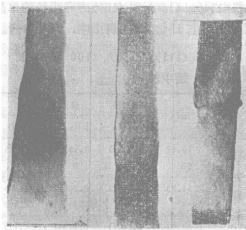
An effective and intuitive way to study this problem is to take the X-ray topography of the longitudinally cut wafer along the growth axis.
 (a)
 (b) Fig. 4: The distribution of dislocations in the two shapes of thin necks. (a) The neck is slightly larger than the seed crystal (b) stretch neck-thin neck
Figure 4 is the projection topographies of two typical thin-necked wafers. From the data in Table 1, where $D_0$ is the seed diameter and $D$ is the radius of the thin neck, it can be seen that when the fine neck diameter is smaller than that of the seed, the distance of error elimination at the fusion surface is consistent with the maximum extended projection distance. When $D > D_0$, $L$ is about 2 times of $L_{\text{emax}}$ d, which may be related to the proliferation of dislocations (see figure 4a) and the fluctuation of thin neck diameter, but it can also be inferred that not pulling the neck is disadvantageous to the exclusion of dislocations.
From the simple analysis of figure 3, it can be seen that the dislocation slip on the inclined $\{111\}$ plane can make the $L_{\mathrm{Emax}}$ smaller, while climbing along the CD direction will increase the $L_{\mathrm{Emax}}$, and climbing along the DC direction will make the $L_{\mathrm{Emax}}$ smaller.
Sometimes dislocations can be eliminated without pulling neck-thin neck slowly. Schwuttke believes that the crystal drawing speed is fast enough so that the supersaturated vacancy concentration is very high, and the dislocation climbs outward, which means that the dislocation climbs to the direction of DC, which indicates that the vacancy moves towards the melt. In recent years, it has been found that the extension and elimination of dislocations in thin necks are also related to the type and concentration of doped elements.
b) Facet growth of dislocation-free Silicon single Crystal It is generally believed that silicon single crystal is grown by the mechanism of two-dimensional surface nucleation and lateral layered growth. When there is a dislocation outcrop on the two-dimensional surface, especially the screw dislocation outcrop, they become the main center of the two-dimensional surface nucleation, which requires less undercooling, while the two-dimensional surface nucleation without dislocation outcrop requires a larger undercooling. What we are
concerned about now is what the two-dimensional surfaces are and their distribution on solid-liquid interfaces of different shapes.
 (a)
 (b) Fig. 5: X-ray projection topography of (11-2) wafer including bract region cut from dislocation-free silicon single crystal deviating from long bract, MoK radiation
Figure 5 shows a projection topography of a dislocation-free silicon single crystal that deviates from the growth of [111], including the "bud" region (11-2). As can be seen from the diagram, the "bud" region has no contrast in the (2-20) phase diagram. however, it has a strong contrast in the (111) phase diagram, due to the value of $\mathbf{g},\mathbf{s}$ is
- [111]/3·[111] = 1 maximum contrast.
- [111]/3·[2-20] = 0 No contrast
According to this contrast change, it can be concluded that the stripe in the "bud" region is parallel to the (111) plane, and its maximum strain direction is [111], in other words, the facet is (111) plane. The highest point of the intersection between the plane and the cylinder is farthest from the high temperature, and the degree of undercooling is the highest. The two-dimensional surface nucleation occurs preferentially here, advances along the (111) plane, and then continues to form a step-like growth front along the solid-liquid interface.
c) Destruction of dislocation-free silicon single crystal growth [9] In the process of dislocation-free silicon crystal growth, dislocations are often caused and multiplied for some reasons. this phenomenon is called the destruction of dislocation-free silicon single crystal growth. In practice, several phenomena of "Lepao", "parabola" and "crystal transformation" are often observed, which are briefly discussed below.
## i. "Lebao"
It is pointed out that when the single crystal deviates from the orientation, it is found that the "Grow out of bao" phenomenon may begin to appear in the fine neck when the dislocation density is reduced to the order of $10^{2} / \mathrm{cm}^{2}$, so the "Grow out of bao" is regarded as a representation of dislocation-free ( $< 10^{2} / \mathrm{cm}^{2}$ ) in silicon single crystal or at least in a certain region of single crystal. On the contrary, in the process of dislocation-free single crystal growth, due to some gradual factor. For example, the small fluctuation of the thermal field leads to the introduction of dislocations in the crystal growth process. It gradually increases, and when the dislocation density increases to more than $10^{3}$, the "bao" will disappear again, which is called the "retrenchment" phenomenon in some production plants, indicating the destruction of the growth of dislocation-free silicon single crystals. In practice, we have observed that the slag consumption in the Czochralski method and the discharge ignition in the zone melting will introduce a large number of dislocations, resulting in "strangulation", and the introduced dislocations will return to the original dislocation-free part, which is obviously a sudden reason.
Whether it is the cause of sudden or gradual change, the observation results of the phenomenon of "lashing the bract" (disappearance of the bract region) all show the end of the small plane growth process, which further shows that the facet growth of silicon single crystal is related to dislocation-free and low-dislocation $(< 5 \times 10^{2} / \mathrm{cm}^{2})$.
## ii. "Parabola" and "crystal transformation"
Twinning may occur in the inclined $\{111\}$ plane during crystal growth. If the twinning of the inclined $\{111\}$ plane occurs, an elliptic curve appears on the surface of the crystal rod, which is called "parabola" in some factories. After the oblique [111] twinning occurs in the $< 111>$, $< 110>$ and $< 100>$ oriented rods, the orientation of the twin rods is $< 115>$, $< 114>$ and $< 221>$, respectively. Because the orientation of the twin is different from that of the main crystal, the requirements for thermal field and other conditions for crystal growth are different, so the defects of the crystal after tilting $\{111\}$ twin are much larger.
In other words, the growth of dislocation-free bodies is destroyed and fewer dislocations become multiple dislocations. Figure 5 shows the projection topography of a $< 111>$ oriented silicon single crystal including the host crystal and the crystal cut wafer after (11-1) twinning. Due to the use of (11-1) reflection, both the main crystal of [111] orientation and the twins of [115] orientation participate in diffraction. It can be seen that the integrity of the crystal is much worse than that of the main crystal.
If the inclined twins occur one after another, especially when several groups of inclined $\{111\}$ planes occur, the thermal field is not suitable for the single crystal.
The growth of, therefore, the emergence of polycrystal, this is commonly known as the so-called "crystallization" phenomenon.
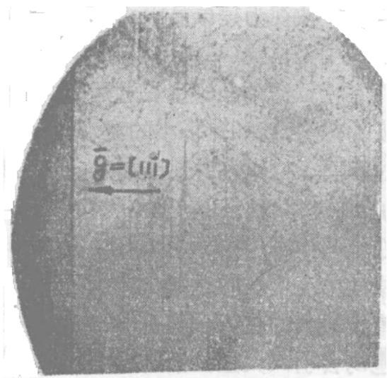 Fig. 5: Shows the projected topography of the two crystals with different integrity after the "parabola".
## iii. Edge exchange and dislocations on twins
In the growth of (111)-oriented silicon single crystals, there is sometimes a sudden position change of 180o in the long edges, and it is obvious that there are two crystals, commonly known as "edge exchange". We cut the (11-2) wafer with two parts of the crystal and take a series of reflection phase diagrams of (333) mt, (202) t and (202) m. According to the analysis, it is concluded that the mechanism of "prismatic exchange" is a twin of a nearly horizontal (111) plane. In terms of its atomic model, the crystal on both sides of the twin plane moves a fraction of the distance between atoms in the direction of the twin. In terms of orientation relation, it rotates $180^{\circ}$ relative to the line of the twin plane. The orientation relation is shown in figure 6(d), which is also proved by Laue orientation. After face exchange, the growth direction of the twin is the same as that of the main crystal. Under the same growth conditions, the two crystals can be dislocation-free or dislocation-free, indicating that "edge exchange" does not necessarily destroy the growth of fault-free silicon single crystals.
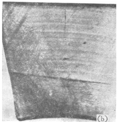
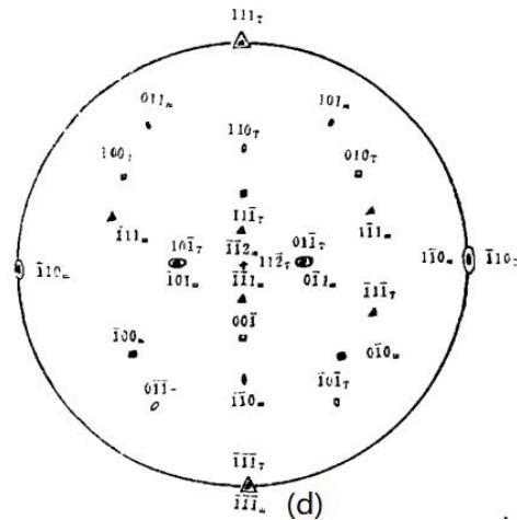
 Fig. 6: The projected topographies of the "edge exchange" chip. (a) (111) reflection, (b) (333) reflection, (c) is the amplification of (b); (d) orientation relationship between main crystals and twins (a)
 Fig. 7: Analysis of the dislocation configuration on the crystal plane in
(a) Spatial relationship, (b) Polar graph analysis
Two groups of dislocation lines are observed on the twin band of figure 6 (a). The angle between them is about $60^{\circ}$ and is divided equally by the [1-10] direction. According to the relationship between the diffraction geometry and the crystal orientation (see 36.7a), the direction of the third-order diffraction (333) of the used (111) is almost parallel to the(11-1) plane, while the twin plane (111) is perpendicular to the(11-2) wafersurface. The dislocation line direction are [10-1] and [01-1] on the (111) plane, they are projected into $60^{\circ}$ on the (11-1)plane. And it is divided equally, as shown in figure 6b, it can be seen that the trends of the two groups of dislocation lines are[10-1] and[01-1] respectively.
### d) Dislocation return and closing process
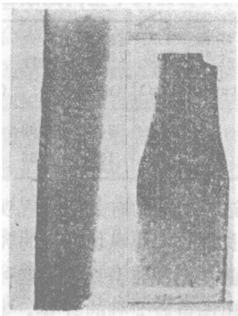
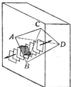
As mentioned earlier, when dislocations are suddenly introduced during crystal growth, these dislocations will return (or reverse extend to the dislocation-free crystal). If twinning occurs, the return of the dislocation in the twin will terminate at the twin plane, as shown in figure 8.
Even if the dislocation-free silicon single crystal grows to the tail, the rapid cooling of the crystal from the melt and the rapid crystallization of the droplet melt bonded with the tail will cause great thermal stress, resulting in a large number of dislocations and slip dislocation bands in the crystal. As shown in figure 8 A, this kind of dislocation will also return to the adjacent dislocation-free single crystals, reducing the yield of dislocation-free single crystals. Similar to the dislocation extension considered previously, the way to overcome this problem is to control the small tail or imitate the tapered ending process of zone melting, which is shown in Fig. 9(a) and (b) respectively. The latter has been successful in the process. For crystals with $< 111,110>$ and $< 100>$ orientations, the angles are less than $39^{\circ}$, $109^{\circ}$ and $91^{\circ}$, respectively.
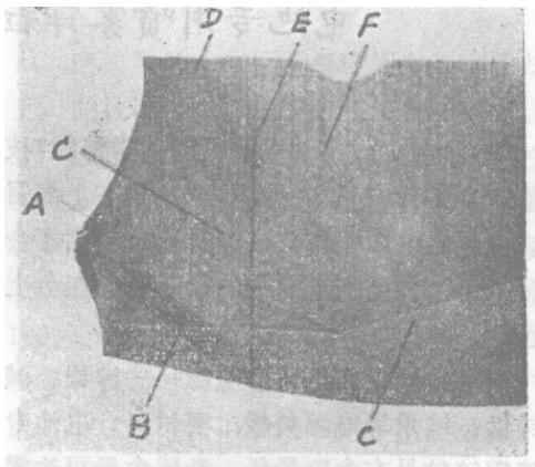 Fig. 8: X-ray projection topography returned by the error at the end of the crystal;
- A is the long-range stress field caused by the rapid crystallization of the final melt.
- B is the introduced slip dislocation band. In addition, it also shows that the curved dislocation C;
- D is a stacking fault, the twin interface E and the growth band F
 (a)
 (b) Fig. 9: Two finishing processes for overcoming the error return of single crystal tail
The above study is only for $< 111>$ oriented Czochralski silicon. In fact, for $< 100>$ oriented Czochralski silicon, the thin neck process and ending process are similar. The failure of dislocation-free single crystals also has "Lepao" and "parabola" phenomena, and the probability of parabola phenomenon is $25\%$ higher than that of $< 111>$ orientation, this is because there are four {111} planes with $54.5^{\circ}$ with (100) faces. However, there will be no "edge exchange".
## V. OBSERVATION AND ANALYSIS OF DEFECTS IN FLOATING ZONE SILICON SINGLE CRYSTALS [10~14]
### a) Defects in grown crystals
The growth of silicon single crystals by floating zone method is mostly carried out in argon-hydrogen mixed atmosphere. In the crystal drawing process, the content of hydrogen in the atmosphere is a very important parameter, so it is necessary to study this problem.
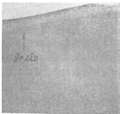
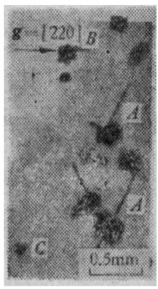
The X-ray appearance of the zone fused silicon (111) wafer grown in argon-hydrogen mixed atmosphere is shown in figure 10. Three types of defect images can be seen, namely, rod pair A, flake B and point pair C. most of the axes of the first two defects are parallel to the intersection line between the $\{111\}$ plane and the wafer surface, and other orientations are also observed. as shown in figure 10, they are the projection of $< 112>$ direction on the $\{111\}$ plane.
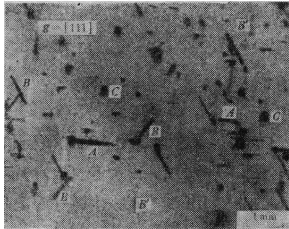 Fig. 10: X-ray topography of single crystal wafers containing $25\%$ hydrogen in atmosphere, MoK $\alpha$
In order to study the effect of hydrogen content in atmosphere, under the condition that other growth conditions are basically the same, a series of oriented single crystals are prepared by changing the flow rate of argon and hydrogen, and the 15mm-length segments and 400um wafers are cut in the same part of the single crystal. After grinding and cleaning, the former is polished in the same container, and the pit density is measured sideways. The dislocation pair density of the wafer was observed after mechanochemical polishing and selective etching, and the projection phase diagram was taken to observe the total bulk density of the three kinds of defects. the relationship between the results and the hydrogen content in the atmosphere is drawn in figure 11. it can be seen that there is a maximum value on the curve, and the peak position is almost all at the hydrogen content of about $10\%$. When the hydrogen content is less than $10\%$, the defect density increases rapidly with the increase of hydrogen content. When the hydrogen content is $10\%$, the defect degree decreases slowly with the increase of hydrogen content. When the hydrogen content is more than $50\%$, there is almost no such defect.
### b) Heat treatment effect of Silicon single Crystal in hydrogen-Argon mixed atmosphere
Fig. 12 shows the X-ray topography of the polished wafer with a thickness of about $400\mu \mathrm{m}$ before and after heat treatment. the comparative observation shows that after annealing at $1200^{\circ}\mathrm{C}$, the contrast of the flake defect image almost disappears, while the rod still has a weak contrast to the defect image. however, almost all the point-to-defects are retained, and the image is dispersed, which seems to correspond to the outward movement of dislocation pairs during processing.
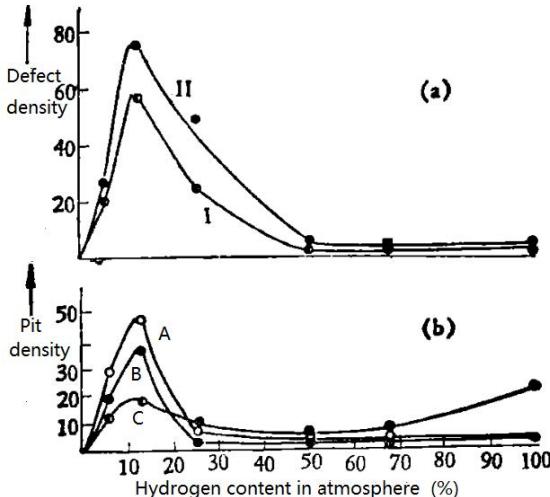 Fig. 11: The relationship between the defect density and the hydrogen content in the growth atmosphere (a) the dislocation alignment I $(\text{pair} / \text{cm}^2)$ of the grown crystal and the defect II $(/\text{cm}^3)$ in the phase diagram; (b) the pit density $\text{cm}^2$; A-represents the growth state, and B and C represent the near-surface and bulk defect density of the crystal segment annealed at $1200^{\circ}\text{C}$ for 11 hours, respectively.
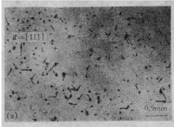 figure 6.
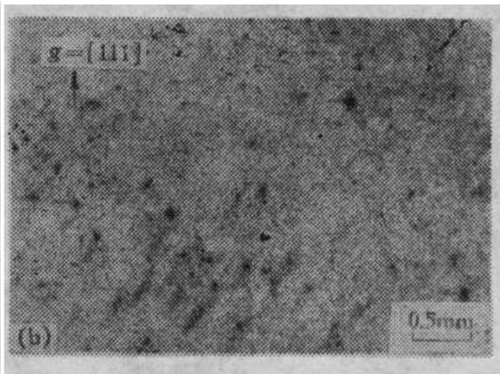 Fig. 12: X-ray topography of the same wafer with 1 before annealing (a) and 6 hours after $1200^{\circ}\mathrm{C}$ annealing
The aforementioned crystal section was annealed at $1200^{\circ}\mathrm{C}$ for 11 hours after grinding and cleaning, then cooled to $600^{\circ}\mathrm{C}$ with the furnace, the oxide layer was removed and polished, the chemical polishing was carried out, the pit density near the surface layer was observed, and then the crystal segment was cut off at half the length, and then the pit density in the body was measured by grinding and chemistry. the results are also shown in figure 11. C three curves show that the pit density near the surface layer is lower than that in the growth state, and the peak position of the maximum value remains unchanged. However, in the body, when the hydrogen content is less than $25\%$, the pit density is lower than that in the growth state, but when the hydrogen content is more than $25\%$, the pit density in the body is generally higher than that in the growth state, and a maximum occurs when the hydrogen content is $100\%$. The results of the research on such defects are described below.
### c) Defects in Silicon single crystals grown in Pure hydrogen atmosphere
## i. X-ray topographic observation
Figure 13 shows the X-ray topography of (111) wafer in pure hydrogen zone melting single crystal after annealing at $1000^{\circ}\mathrm{C}$ for 1 hour. rod pairs, single rod and point defects are obtained, rod defect point to $< 1 - 10>$ direction and quite long scale are also observed. they have strong contrast in the topography of $\{2-20\}$ symmetric diffraction geometry or $\{11 - 1\}$ asymmetric diffraction, indicating that they do not have, $< 11 - 2>$ or $< 1 - 10>$ strain vectors.
 (a)
 (b)
 (c) Fig. 13: X-ray topography (a) (b), (c) optical micrographs of single crystals grown in pure hydrogen after annealing at $900^{\circ}\mathrm{C}$ for 1 hour
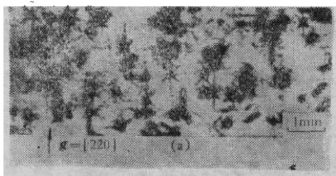
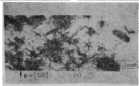 Fig. 14: X-ray topographies of single wafer annealed at $1000^{\circ}\mathrm{C}$ for 1 hour in pure hydrogen atmosphere
Fig. 14 shows the topographies of the(001),(1-10) and (111) wafer cut from the same single crystal after being treated at $1000^{\circ}\mathrm{C}$ for 1 hour, and the image of "rose knot" defect emitted from a strain center can be observed. In the topography of the (001) wafer, see figure 14 (a). In addition to the two groups of intersecting marks (1-10) and [110] parallel to the $\{111\}$
plane and the surface, we can also see two groups with $45^{\circ}$.
In the topography of the (111) wafer, in addition to the [1-10], [01-1] and [10-1] three groups, we can also see the three groups that form $30^{\circ}$. See figure 13 (c) synthesize the projection relationship of the "rose knot"-like defects in the three kinds of chip projection phase diagrams, it can be inferred that a complete "rose knot" defect is composed of twelve rose petals in the $< 112>$ direction. From the picture with higher magnification, 14b, you can see. A rose petal consists of a row of dislocation loops, and there is a complex structure of multiple central rings near the strain center.
In order to determine the Boolean vector of the dislocation ring array, a series of symmetrical and asymmetric transmission geometric diagrams of the (111) wafer are photographed. According to the law of image elimination, it is found that the dislocation ring array has a Burgers vector parallel to its petal axis
$< 110>$, which is consistent with the results of Cui Shufan et al.
## ii. Secondary annealing effect
The topographies of the wafer cut on the wafer annealed at $900^{\circ}\mathrm{C}$ for 1 hour before and after secondary annealing is shown in figure 15, which is obviously different from that shown in figure 12, indicating that secondary annealing can not reduce and eliminate the defects produced during the first annealing.
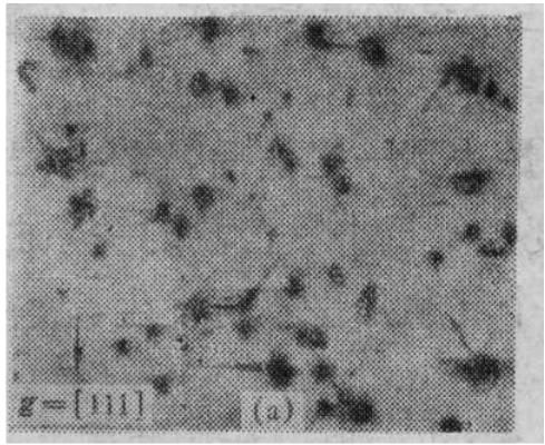
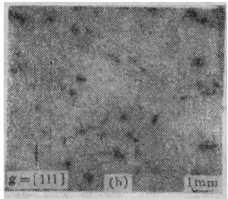 Fig. 15 (a): The topography of the wafer cut from the hourly segment annealed at $900\mathrm{C}$; (b) the topography of the same wafer annealed at $1100^{\circ}\mathrm{C}$ for 4 hours
### d) Precipitation of hydrogen in single crystals and the mechanism of hydrogen-induced defects
From the above experimental results, the existence of these hydrogen-induced defects is closely related to the state of hydrogen in single crystals. The solubility of hydrogen in melt silicon is large, and the hydrogen entering into freshly grown silicon through the melt is of the order of $2 \times 10^{19} / \mathrm{cm}^3$, while the solubility in solid silicon is very small, as shown in Table 1. except for the partial outward diffusion during the cooling process of crystal growth, if the cooling rate of the crystal is fast enough, then the rest of hydrogen is dissolved in the crystal by interstitial supersaturation, which is proved by the infrared absorption spectrum of silicon single crystal in floating zone in pure hydrogen atmosphere. If the crystal is cooled slowly enough, or if the crystal is cooled fast enough, the supersaturated solid solution hydrogen will dissolve and precipitate. Jiang Bolin et al. [9] studied the floating zone silicon single crystal treated by $500\sim 1000^{\circ}\mathrm{C}$ at different temperatures for 1 hour by X-ray face center method. It is considered that it is first the decomposition of Si-H bond, then nucleation and growth by diffusion, and the precipitate changes from spherical to elliptical disk, and the precipitate is parallel to $\{111\}$ plane. When the stress at the interface between the precipitate and the matrix exceeds the yield stress of the silicon at the treatment temperature, the dislocation ring is emitted in its favorable direction, as can be seen in figures 14 and 15, the multi-center dislocation ring of the complex structure near the high contrast region of the core and the dislocation ring far from the core.
Table 1: Solubility of hydrogen in silicon at different temperatures [10]
<table><tr><td>temperatures (°C)</td><td></td><td colspan="2">Two kinds of calculation results</td></tr><tr><td></td><td>%</td><td>Atoms/cm3</td><td>Atoms/cm3</td></tr><tr><td>500</td><td></td><td></td><td>3.4x109</td></tr><tr><td>1000</td><td>3.6x10-6</td><td>1.8x1014</td><td>2.0x1014</td></tr><tr><td>1200</td><td>4.0x10-6</td><td>1.8x1015</td><td>2.4x1015</td></tr><tr><td>1300</td><td>1.7x10-5</td><td>8.5x1015</td><td>4.8x1015</td></tr><tr><td>1400</td><td>5.3x10-5</td><td>2.7x1016</td><td>1.2x1016</td></tr><tr><td>1420 (liquid state)</td><td>0.45x10-1</td><td>2.3x1019</td><td>1.3x1016</td></tr></table>
The emission mechanism of the dislocation ring is shown in figure 16. A group of flake precipitates on the $\{111\}$ plane can emit the dislocation ring by prism stamping in three favorable $< 110>$ directions. The primitive ring consists of two pairs of dislocations parallel to each other, each on a set of parallel slip planes, and the direction of the dislocation is $< 112>$. The two pairs of dislocation lines have the same Burgers vector and are parallel to the intersection of the two slip planes. The size of the initial dislocation ring is closely related to the projection scale of the precipitate in the emission direction. If the precipitates are on several groups of $\{111\}$ planes at the same time, or when the precipitates are almost spherical, the dislocation rings can be emitted to $12 < 110>$ directions to form a "star" dislocation ring array, as shown in figure 14. At high temperature, under the action of continuous emission stress, the dislocations of the dislocation rings move along the common slip direction on their respective slip planes, and the emission core slip continues one after another, so that the dislocation rings are arranged in strings along the emission direction. The dissonance of the slip of dislocation rings on each plane and the interaction of climbing nuclei make the dislocation rings of different sizes on one row distorted. As a result, multiple central dislocation loops with complex configurations are formed near the core.
 (a)
 (b)
 (c) Fig. 16: A schematic diagram of the dislocation ring emitted by a flake hydrogen precipitate. ABCD is a regular tetrahedron composed of {111} faces. If the precipitate is parallel to ABD, the emission direction of the dislocation ring is (a) AC direction; (b) BC direction; (c) CD direction.
The experimental results show that all crystals with this defect, especially those with high defect density, can not produce qualified devices, and serious local breakdown will occur. However, it is worth mentioning that when the floating zone silicon single crystal grown in pure hydrogen atmosphere is cut into $700\mu \mathrm{m}$ thick wafers and heat treated as mentioned earlier, there are no defects such as hydrogen precipitated nucleus dislocation ring array. This may be due to the outward diffusion of hydrogen during heat treatment rather than the accumulation and precipitation in the wafer.
## VI. MICRODEFECTS AND VORTEX DEFECTS IN DISLOCATION-FREE SILICON SINGLE CRYSTALS [15,18]
Practice shows that although the scale of vortex defects is small, silicon wafers are very easy to cause oxidation stacking faults due to the influence of stress field in the process of thermal oxidation, which has an important impact on silicon devices, so it is necessary to study this problem.
The methods of observing and studying microdefects and behavior defects in dislocation-free silicon single crystals are as follows: one is the etching method for polishing wafers, and the commonly used etching agent is HF: $33\% \mathrm{CrO}3 = 1:1$. The practice shows that the etching effect of cutting and polishing wafers for growing crystals is not good, and it is often necessary to carry out 1100oC wet oxygen oxidation and then etch them. Similarly, the effect of direct observation of growing crystals by X-ray appearance method is not good, and it generally needs to be decorated with copper before the effect is observed
There are micro defects in dislocation-free silicon single crystal, which are thermal vacancy, interstitial atoms and chemical impurity atoms will be supersaturated under certain conditions and will be condensed into point defect clusters, which are called micro defects. Vortex defects are micro-defects in the macroscopic distribution of vortex. Microscopically, vortex defects and dislocations also form triangular corrosion pits, the difference is that the micro-defects are triangular shallow flat-bottomed corrosion pits with a white core under the microscope and a small scale. The dislocation is a deep sharp-bottomed etching pit, which shows a black triangle under the microscope, as shown in figure 17.
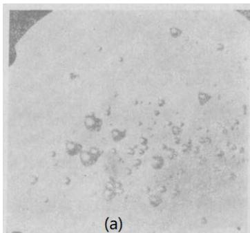
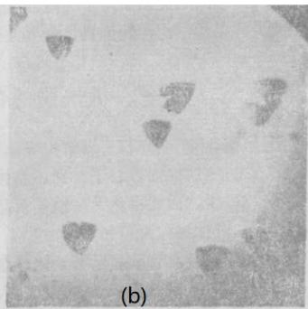 Fig. 17: Etching pits for microdefects (a) and dislocations (b)
Macroscopically, the micro-defects show vortex stripes, as shown in figure 18, and are often decorated with carbon and heavy metal impurities, which are similar to resistivity stripes, but their mechanisms and micro-morphologies are different. The difference is that the essence and formation mechanism are different, the vortex defects are formed by the aggregation of hot spot defects, and the resistivity fringes are caused by the segregation fluctuation of doping elements. Microscopically, the micro-defects are triangular flat-bottomed corrosion pits or Xiaoqiu, the resistivity fringes are micro-corrosion pits, and the corrosion surface is mirror.
The distribution of vortex defects is as follows: there are two shallow etch pits, namely A defect and B defect, An is a large etch pit or mound $(3\mu \mathrm{m})$, B is a small etch pit( $\sim 1\mu \mathrm{m}$ ).
The distribution of A defect is two orders of magnitude less than that of B defect, both of them are striped, but the position of distribution is different. B defect is distributed around the wafer, the center is less, and A defect is distributed in the center of the crystal.
The transverse and longitudinal distribution characteristics of the vortex defects are that when the cutting plane is perpendicular to the growth axis, several levels of corrosion pits are displayed at the same time, forming the vortex stripes shown in figure 19 (b). When the cutting surface is not perpendicular to the growth axis, the cutting surface intersects several levels of the vortex defects, showing each level and an arc segment, as shown in figure 19 (c).
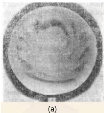
 Fig. 18: Vortex distribution of microdefects
There is no vortex defect in the dislocation-free silicon single crystal, but this behavior defect exists in the dislocation-free silicon single crystal, and the concentration of microdefects is low in the $1\sim 2\mathrm{cm}$ range of the crystal surface.
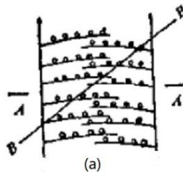
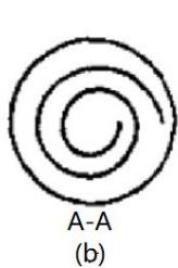
 Fig. 19: Silicon Wafer cutting, Grinding and polishing observation and Analysis
The formation of vortex defects is related to single crystal growth stripes, thermal field symmetry and crystal remelting during growth, so crystal remelting can be avoided by adjusting crystal growth parameters, such as melting temperature, crystal diameter, casting speed and rotation speed, etc. while using a higher casting speed, keep the flat and concave growth interface, so that the vortex defects can be reduced and eliminated.
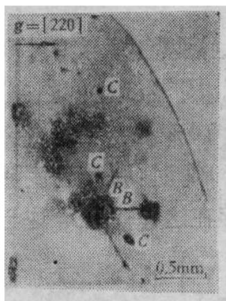
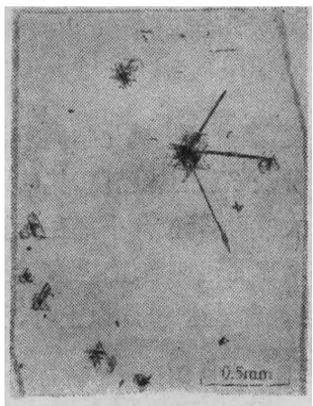
The problem is that when crystals with such vortex defects are annealed by $1350^{\circ}\mathrm{C}$ and come out of the furnace quickly (such as falling to room temperature within 20 seconds), the wafers are oxidized by $1200^{\circ}\mathrm{C}$ for 3 hours, and it is found that in addition to the circular stacking faults of the raw materials, half-ring dislocations are also found, as shown in figures 20 and 21. These paired dislocation loops are divided into two categories, which are represented by A and B. For the (001) wafer, the two A-type semirings are located on the two inclined $\{111\}$ where the surface intersection marks are parallel to each other, and their spatial configuration and projection on the (001) plane are shown in figure 22 (a). The B-type hexagonal dislocation ring is located on two $\{111\}$ planes perpendicular to the surface intersection marks, and its spatial configuration and projection on the (001) plane are shown in figure 22 (b). The projection of the development of the two dislocation rings on the (001) plane is shown in Fig. 23 (a) and (b), respectively. The type A semicircle dislocation is a process of climbing, sliding and cross-slip, while the type B is initially due to the precipitation of the climbing word to emit a circular dislocation ring parallel to the surface, and then transformed into a square ring in the "110" direction. Under the action of decomposition shear stress, a pair of flat dislocations slip in the opposite direction, thus developing into a hexagonal dislocation ring [36].
Similar half-ring dislocations are also found for (111) wafers [37].
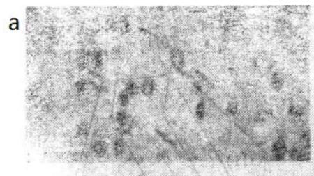
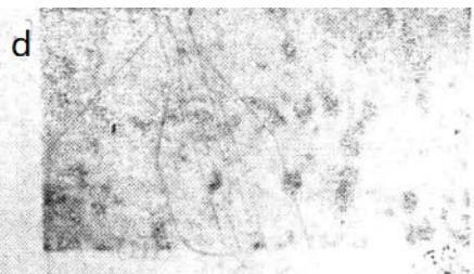
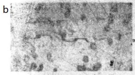
 Fig. 20: The circular stacking faults and half-ring dislocations A & B along the vortex defects and show the different stages of the development of half-ring dislocations.
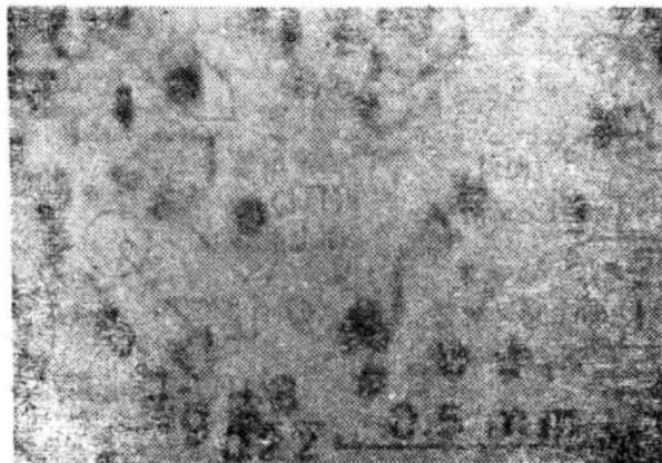 Fig. 21: The circular stacking fault along the vortex defect and the semi-dislocation ring B, (111) wafer on the (111) plane perpendicular to the surface intersection mark
 (a)
 (b) Fig. 23: Projection of dislocation configurations in the formation, development and multiplication of two semi-dislocation rings A (a) and B (b) on the (001) plane (1) (2) (3) a 0 (4) [110](5) Slip on (1-11) plane Slip on (1-11) plane (6) m 1 (7) [101] d j Slip on (1-11) plane (8) $f$ Slip on (-111) plane (9)p (10) (b)
Fig. 22: Spatial configuration of two kinds of semi-dislocation rings and projection on (001) plane. (a) A-type semi-dislocation ring pair (b) B-type semi-dislocation ring
(3)
(4)
Slip on (-1-11) plane 2 Slip on (111) plane
## VII. TEST AND ANALYSIS OF DIRECTIONAL CUTTING AND POLISHING PROCESS OF WAFER
The first step in the process is to make a reference surface. In the early days, the first step was to circle the grown silicon single crystal which was close to the cylinder, so that the wafer cut perpendicular to the growth axis was an ideal circle. From a modern point of view, this is necessary and wrong, because the rolling circle loses the reference of the crystal orientation relation, which makes it difficult to make the reference plane. Secondly, the rolling circle inevitably leaves residual stress on the crystal surface, resulting in some kind of stress concentration. It makes the wafer easy to slip dislocation in the later thermal process, which affects the yield and yield of the device. The round rolling process can be completely discarded.
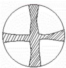
The growing crystal bought by the device maker may be an entire ingot or an ingot that has been cut into segments. Whether it is $< 100>$ orientation or $< 111>$ orientation, the end face needs to be ground with thicker sand for optical orientation. The light reflection patterns of the three oriented crystals are shown in figure 24, which shows that they are four times, three times and two times symmetrical. Referring to this pattern, or referring to the growth edge of the ingot surface to make the reference plane, is to grind a certain orientation plane on the crystal surface. The method is:
(1) For the crystal end of $< 100>$ orientation, the reference plane should be strictly parallel to the line of the diagonal edge, or parallel to the cross line of reflected light. (2) For the $< 111>$ oriented crystal segment, the reference plane should be strictly parallel to the line of two growth edges or parallel to the line of three light spots. If you think about it, the method of reference growing edges is more accurate.
 \<100>
 \<111>
 \<110> Fig. 24: Cross-sectional light reflection images of crystals with three orientations: $<100>$, $<11>$ and $<110>$
The second step is directional cutting, which is to install the crystal segment on a special fixture with three-degree rotation for orientation, and carefully adjust the three-degree rotation to make the strictly symmetrical reflected light pattern appear to start cutting. For general requirements, this is fine. However, some requirements are not roughly $< 100>$ or $< 111>$ oriented wafers, but wafers that deviate several degrees from a specific orientation, so it is necessary to cut out a piece and then proofread it with an X-ray orientator. determine how to adjust in order to achieve the required adjustment parameters, according to this adjustment parameter and then carefully adjust before cutting. The cut wafer not only has a clear reference edge, but also can see the growth edge of the wafer edge.
The third step is the strict and meticulous grinding and polishing of the wafer. Polishing generally leads to the use of mechanochemical polishing. We are concerned about the test and analysis of grinding damage here to determine whether polishing has removed the grinding damage. The testing methods are as follows:
## i. The method of measuring diffraction intensity
The sample to be measured is processed into a strip as shown in figure 21 (a). The new cutting surface is chemically polished to remove the surface damage, and the relative intensity of the transmitted diffraction line is measured according to the diffraction geometry shown in figure 25 (a). Because of the damage on the machined surface, the diffraction intensity distribution shown in figure 25 (b) can be obtained. When the diffraction intensity decreases to a constant value, the distance to the machined surface is the thickness of the damage layer.
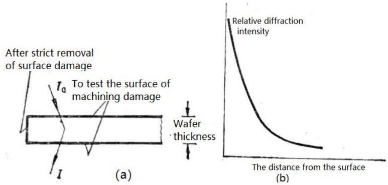 Fig. 25: Diffraction intensity method for measuring damage of silicon wafers
## ii. Take the appearance diagram of the cleavage plane
- In order to avoid the treatment of new cutting, the desired sample can be obtained by cleavage, and the projection phase diagram can be taken, which can be determined by observing the contrast change from the machined surface to the interior of the crystal. iii. The half width method of the double crystal swing curve
It has known that when the dislocation density of the crystal is greater than that of $10^{3} / \mathrm{cm}^{2}$, the half width of the double crystal swing curve increases with the increase of the dislocation density, which indicates that the half width of the double crystal swing curve is sensitive to the damage to the wafer. In one method, the half width of double crystal swing curve obtained by different processing methods of the same batch of wafers is observed for qualitative comparison; in another method, the half width of double crystal swing curve is observed after etching and delamination in different time, and the relation curve between half peak width and delamination depth (or corrosion time) is obtained. When the half peak width reaches a constant value, it is the thickness of the damage layer. Table 2. A typical measurement result is given.
Table 2: Determination of damage layer of Silicon {111} {100} Wafer cut in Grinding
<table><tr><td rowspan="2"></td><td colspan="2">\{111\}wafer, (111) diffraction</td><td colspan="2">\{100\}wafer, (400) diffraction</td></tr><tr><td>Outermost half width/second</td><td>Depth of damage layer / \mu m</td><td>Outermost half width/second</td><td>Depth of damage layer / \mu m</td></tr><tr><td>Cut wafer</td><td>146.6</td><td>18~20</td><td>64.4</td><td>18~26</td></tr><tr><td>Grinding wafer</td><td>91.2</td><td>~6</td><td>30.4</td><td>~5</td></tr></table>
## VIII. STUDY ON OXIDATION PROCESS
Oxidation is a very important process for silicon integrated devices, especially the first oxidation, which is not only a test of wafer processing quality, but also a method to explore a better oxidation process. It was the 1970s, when China was in the midst of a chaotic cultural revolution, when several of us young people carried out an exploration of silicon wafer oxidation process behind our backs. After the establishment of the oxidation stacking fault display by etching method, we began to explore the process to reduce the oxidation stacking fault. For this reason, the following comparative experiments were carried out. That is, the same polished silicon wafer is oxidized by different methods. 1) direct wet oxidation; 2) vacuum (or protective atmosphere) annealing for 0.5 hours at the same temperature, and then wet oxygen oxidation for the same time; 3) dry oxygen oxidation for half an hour and then wet oxygen oxidation. And keep the oxide thickness of the three kinds of silicon wafers roughly the same.
After the oxidation stacking fault measurement, it is concluded that the oxide stacking fault density of direct wet oxygen oxidation is the highest, followed by dry oxygen oxidation followed by wet oxygen oxidation, and the oxide stacking fault density of first annealing followed by wet oxygen oxidation is the lowest. This shows that the polishing damage of annealed wafers can be eliminated to a certain extent.
In order to confirm the nature of the oxide stacking fault, the oxide stacking fault was deliberately grown, and then studied by X-ray diffraction. The results show that the stacking fault plane is $\{111\}$ plane which is inclined to the wafer, the stacking fault vector Renz1max $3 < 111>$, and the boundary of the stacking fault is a prismatic dislocation ring. Therefore, there are three groups of oxide faults forming $120^{\circ}$ each other on the $\{111\}$ wafer, which are respectively located on the $\{111\}$ plane of $70.5^{\circ}$ with (111), and on the second (100) wafer, there are two groups of oxide faults of $90^{\circ}$ each other, which are respectively located on the four $\{111\}$ planes of $54.5^{\circ}$ with (100).
## IX. EPITAXIAL PATTERN DISTORTION [20~23]
Drum and Clark [20] found that when the orientation deviation is less than 0.50, the epitaxial pattern of the wafer is seriously distorted and diffuse, which makes it difficult to carry out the subsequent lithography. Bean et al. [21] proposed that the deviation from $2\sim 4^{\circ}$ to the nearest (110) can minimize the distortion. In practice, we find that when the reference plane of the wafer is (1-10) and the wafer orientation (110) deviates from $2\sim 4^{\circ}$, the lines perpendicular to the reference in the buried pattern become wider obviously. therefore, we study the relationship between the pattern micro-distortion and the deviation orientation in this deviation range.
Taking the growth edge of silicon single crystal as the reference plane (1-10), the X-ray Laue directional cutting is used to cut the wafer $\{100\}$ and the nearest $\{110\}$ to the wafer which deviates from $2\sim 4^{\circ}$, see figure 26. according to the general bipolar circuit turn-on isolation process, the pre-epitaxial processes are completed, and the lithography patterns are arranged parallel to the reference edge and $60^{\circ}$ with the reference edge, and then $1200^{\circ}\mathrm{C}$.
The epitaxial growth is made, and the thickness is about 4 microns. Finally, it is observed by interference contrast microscope. The results are as follows:
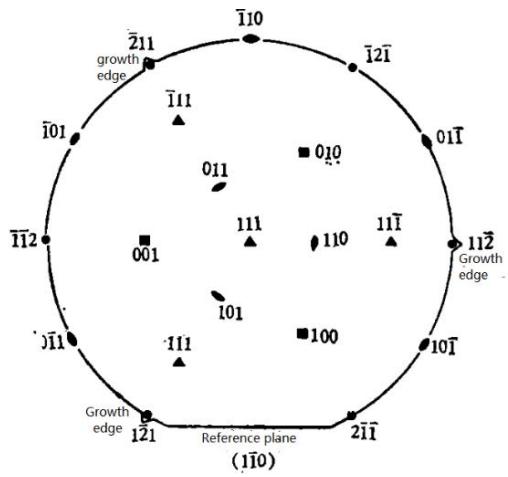 Fig. 26: A simplified stereographic projection of the orientation relationship of the wafer, and shows the reference plane and growth edge
## i. Wafers deviated from (110) and (001)
When the figure is arranged parallel to the reference edge, the line perpendicularly to the reference edge is obviously asymmetrically broadened, and its relative width reaches $\sim 66\%$, as shown in figure 27 (a) (b). For the wafer deviated from (110), if the figure is 60o with the reference edge, the scale of the two lines perpendicular to each other is almost unchanged, only chamfering occurs at the intersection of them.
## ii. Wafer deviated from (011) or (101).
In order to further prove the phenomenon of Cookie change of wafer patterns deviated from (110), similar experiments have been carried out on wafers deviated from (011) or (101). The results show that when the patterns are arranged parallel to the reference edges, the scales of the two lines perpendicular to each other are almost unchanged, as shown in figure 27 (b). When the figure is 60o with the reference edge, only the lines perpendicular to the projection of the normal of (011) or (101) appear broadening [23].
## iii. Wafer deviated from (100) or (010)
When the graphics are arranged parallel to each other, the two lines perpendicular to each other are obviously narrowed, as shown in figure 27 (d).
To sum up, it can be seen that the degree of pattern distortion is closely related to the orientation of lithography steps, which may be due to the epitaxial growth of lithography steps. Two-dimensional nucleation plays an important role in lateral growth, and the anisotropy of lateral growth rate is the cause of pattern distortion.
In order to minimize the micro-distortion of the epitaxial pattern, the (111) wafer should not deviate $4^{\circ}$ from the nearest (110) when the reference plane is. Instead, it should deviate $2^{\circ} \sim 4^{\circ}$ from the nearest (011) or (101), that is, not around the axis perpendicular to the reference edge (110).
 (a)
 (b)
 (c)
 (d) Fig. 27: Interference contrast micrograph of micro-distortion of Eagle (111) wafer during epitaxy [23], the pattern is arranged parallel to the reference edge [112]. (a) deviate from $2^{\circ}$ to (110); (b) deviate from $4^{\circ}$ to (100); (c) deviate from $4^{\circ}$ to (101); (d) deviate from $4^{\circ}$ to (010)
Deviate, but should deviate from the axis (011) or (101) of the reference edge $30^{\circ}$. This process has been used in the development of ECL-1K and TTL-K bipolar large-scale integrated circuits with good results.
It should be noted that the reference plane (1-10) should not be, but should be (11-2), that is, the $< 1 - 10>$ direction, which ensures the highest wafer yield. However, it is no problem to deviate from $2\sim 4^{\circ}$ to the nearest (011) or (101), or even to the nearest (110). However, the long edge of the circuit graph should be parallel to the reference edge, that is, along the [1-10] direction.
## X. X-RAY TOPOGRAPHIC OBSERVATION AND STUDY ON THERMAL PROCESS TRACKING OF SILICON INTEGRATED DEVICES
Practice has proved that a certain crystal defect and density can reduce the breakdown voltage of semiconductor devices, increase the leakage current and produce excessive noise, thus reducing the yield of semiconductor devices. Because of the non-destructive and area-reaching imaging advantages of X-ray topography method, useful results can be obtained in studying the relationship between induced defects and device yield, as well as the generation and elimination of induced defects and improving the device process. At that time, in order to take X-ray appearance pictures of large-diameter wafers, the author, in cooperation with mechanical designers, designed and manufactured a remote-controlled X-ray projection camera capable of shooting two-inch-diameter wafers, and later won the Shanghai third-class Science and Technology Progress Award.
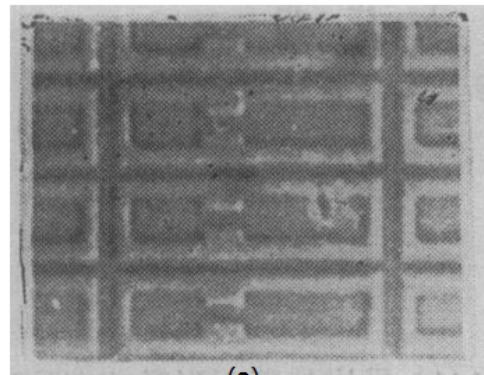
The relationship between the induced defects and the yield can be established by taking the appearance phase diagram of the silicon after wiring and alloying and comparing the distribution of the qualified chips. Fairfied and Schwuttke [24] found that $90\%$ of diodes have hard breakdown in dislocation-free regions and only $20\%$ in dislocation-free regions. Authier et al. [25] found the relationship between dislocations and Zener diode failure. Jungbluth and Wang [26] found an one-to-one relationship between induced slip dislocation bands and the yield of high-power transistors. Schwuttke [27] studied the relationship between large-scale integrated circuits and slip dislocation bands, and obtained the corresponding relationship as shown in figure 28. As can be seen from the figure, the internal yield of the middle region of the wafer without slip dislocation is up to $70\%$, while the unqualified units are clustered in the area with high slip dislocation density, but not all the units there are bad, in which the bad devices may play the role of absorbing impurities. So that some units around it are still qualified, so there is only a statistical corresponding relationship between the induced slip dislocation and the yield. Schwuttke et al. [28] studied N-channel insulated gate field effect transistor devices by the same method and found that there is a good corresponding relationship between the leakage current distribution and the induced stacking fault density. They specify that the leakage current of qualified devices is below 1nA, and the distribution of unqualified devices due to leakage current corresponds to the area of oxide fault contrast in the X-ray topography.
The author has also carried out a "study on the X-ray appearance of device process tracking wafers", that is, each step of the thermal process in the fabrication process of large-scale integrated circuits, such as epitaxy, oxidation, diffusion, etc., carries out a completely non-destructive inspection of the wafers one by one. In this way, the generation and development process of induced defects in wafers can be observed and discovered, thus revealing the causes of induced defects. Finally, the defect distribution in the appearance phase diagram of the wafer is compared with the distribution of the yield on the wafer. Figure 28 also shows.
 (a)
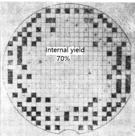 (b) Fig. 28: The corresponding relationship between slip dislocation band and yield of large-scale integrated circuits. (a) The topography after alloying shows the origin. A strong dislocation band at the edge of the wafer; (b) the yield distribution map, and the black square is a substandard device
It is found that there is a good corresponding relationship between the distribution of finished product rate and the distribution of induced slip dislocation zone, which is consistent with the above-mentioned foreign research results.
So ask, why are there still so many qualified devices around the chip? It can be explained as follows that when the device in the slip dislocation zone with precipitated impurities is unqualified due to large leakage, while the device in the dislocation zone without precipitated impurities is qualified.
It is also found that the slip dislocation band starts from the long-range stress field at the edge of the wafer and gradually develops to the center of the wafer, and is related to the large temperature gradient in and out of the thermal process. As a result, three principles for the best thermal process are put forward: 1) after the wafer is cut and round, after the reference edge is made, the long-range stress field should be eliminated by corrosion method before polishing; 2) the wafer should be slowly into and out of the furnace; 3) the wafer should be placed vertically as far as possible in the high temperature furnace. Flatness of the wafer boat should also be paid attention to to avoid large radius wafer bending in the thermal process as far as possible.
## XI. TEST AND ANALYSIS OF WAFER BENDING IN SILICON DEVICE PROCESS
In the thermal process of silicon devices and integrated circuits, they are generally very thin ( $\sim 300$ microns) and large diameter (2 inches or larger) wafers. Bending occurs due to different surface forces; in the high temperature cycle, due to improper placement of the wafer, such as warping of the quartz boat when the wafer is standing or flat, bending is caused by self-weight; or when the wafer comes out of the furnace, the temperature gradient difference between the edge and the center will also cause the wafer to bend; in addition, the epitaxial or diffusion layer mismatch between the substrate will also lead to wafer bending. Because the bending radius of this kind of bending is very large, many quantitative measurement methods fail, and the X-ray profile and double crystal diffractometer methods are very effective, non-contact, non-destructive, and can follow the process for quantitative analysis.
If the wafer curved crankshaft is vertical, that is, parallel to the vertical linear incident ray, then two diffractive contrast images will appear in the projection topography, as shown in figure 29(a) if the recorder is scanned synchronously with the crystal, the two diffraction transmission peaks are recorded, as shown in figure 29 (b) as shown, they correspond to the diffraction at A and B of the same set of crystal planes of the wafer in the incident $K_{\alpha 1}, K_{\alpha 2}$ beam, whose diffraction geometry is shown in figure 30. It is shown that the angle between the two crystal planes at A and B is $2\delta$, the distance is S, and their diffraction angles are $\theta_{1}$ and $\theta_{2}$, respectively.
$$
S/2 = \rho \sin \delta
$$
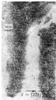 (a)
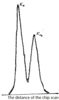 (b) Fig. 29: The projection topography (a) of curved silicon wafers and the intensity distribution of parallel scanning of wafers (b). Both pictures show the diffraction band.
Since $2\bar{\boldsymbol{\delta}} = \theta_{2} - \theta_{1} = \Delta \theta_{2-1}$, it can be obtained from the differential Bragg formula, that is,
$$
\Delta \theta_{2-1} = (\Delta \lambda / 2) \tan \theta
$$
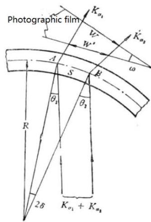
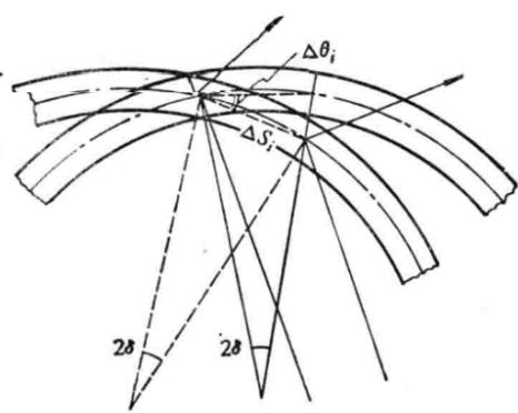 Fig. 30: Diffraction Geometry of uniaxial
Among them, $\Delta \lambda = \lambda_{\mathsf{K}\mathsf{a}2} - \lambda_{\mathsf{K}\mathsf{a}1}, \lambda = (1/3)\times (2\lambda_{\mathsf{K}\mathsf{a}2} + \lambda_{\mathsf{K}\mathsf{a}1})$, When the photographic film is placed parallel to the surface of the wafer, then the distance between the diffraction bands of $\lambda K_{\alpha 2}$ and $\lambda K_{\alpha 1}$ is $t = S$ so the radius of curvature $R$ is
$$
R = t / \left[ 2 \sin \left( \Delta \theta_{2 - 1} \right) / 2 \right]
$$
Because $\Delta \theta_{2-1}$ is very small, $\sin (\Delta \theta_{2-1} / 2) = \Delta \theta_{2-1} / 2$, Therefore, there are
$$
R=\omega/\Delta\theta_{2-1}
$$
Therefore, according to the time distance $t$ between the two diffraction bands on the photographic film or the recording paper, the bending radius $R$ can be obtained. If the negative is placed perpendicular to the diffraction line,
$$
S = t / \cos\omega
$$
Where $\omega$ is the angle of the negative on the surface of the wafer (see figure 31). For symmetrical transmission Laue geometry, $\omega = \theta$, so the formula (7) can be written as
$$
R = \omega / (\Delta \theta_ {2 - 1} x \cos \theta) \tag {9}
$$
In addition, the bending radius can be calculated according to the width of the diffraction band or the base width of the single diffraction peak.
$$
R = L / 2 \varphi
$$
Where $\Phi$ is the horizontal divergence of the incident beam.
The aforementioned method either needs to take the appearance phase diagram, or record the scanning intensity curve when rotating the scanning wafer, and assume that the radius of curvature between $K\alpha_{1}$ and $K\alpha_{2}$ diffraction bands is constant, and the result is the average value in the range of inter-band distance. The author has developed a simple and convenient method for direct measurement. Its diffraction geometry is shown in figure 30. Suppose a certain scanning distance of the wafer is $\Delta S_{i}$, and the corresponding diffraction angle difference is $\Delta \theta_{i}$. According to the derivation of figure 31, $\Delta \theta_{i} = 2\delta_{i}$, the formula can be written as
$$
R = \Delta S_{i} / \Delta \theta_{i}.
$$
The direction of the bending of the wafer can also be observed by using the X-ray phase diagram, which is not detailed here.
## XII. STUDY ON ION IMPLANTATION DOPING OF SILICON WAFER
Ion doping and impurity absorption by ion bombardment have been widely used in the manufacture of silicon devices. X-ray topography is one of the effective methods to study the injection-annealing behavior of injected atoms and damage.
Kishino and Noda [29] studied boron and phosphorus $(1 \times 10^{16} \mathrm{atom/cm}^3)$ implanted into $100 \mathrm{keV}$ with a double crystal diffractometer. They found that the wafer bending after implantation is convex and has nothing to do with the type of implanted reason. The implanted ions are generally in the interstitial position, and the implanted wafers are annealed at different temperatures. It is found that within a certain range of problems, the bending radius and lattice parameters of the implanted boron wafers become larger, indicating that the interstitial atomic fraction of boron increases. On the other hand, the bending radius of the implanted phosphorus wafer becomes smaller and the lattice parameters become larger, which indicates that the part of the interstitial position occupied by phosphorus is smaller, and then the transition occurs. According to the change of the square resistance with the annealing temperature, the turning temperature of boron implanted is $700^{\circ}\mathrm{C}$, that of phosphorus is $600^{\circ}\mathrm{C}$, and the annealing below this temperature is called "reverse annealing". When annealed above this temperature, the lattice parameters of boron implanted wafers become smaller, the resistance becomes smaller, and boron occupies the substitute position. Play the role of electrical activity.
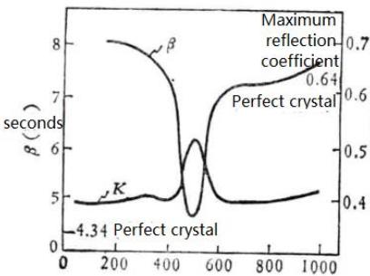
Lecrosnier et al. [30] implanted boron at the energy of $500\mathrm{keV}$ and the dose of $1\times 1015$ atom/ $\mathrm{cm}^3$. The distance between the main peak and the subpeak was measured by double crystal diffraction. The relationship between the diffraction intensity and half width of the main peak and the annealing temperature is shown in figure 32(a) (b). The most obvious feature is that the diffraction intensity and half width of the main peak of $500\mathrm{oC}$ are close to that of the complete crystal, while the subpeak is still very sharp, indicating that the layer between the surface and the implanted layer (about $0.8\mathrm{um}$ thick) is completely restored during $500^{\circ}\mathrm{C}$ annealing, and there is still a lattice strain in the crystal which is larger than the distance between the crystal planes of the substrate. After $600\mathrm{oC}$ annealing, the double crystal layer disappears. This kind of lattice strain is released by producing secondary defects, and the half width of the matrix increases during $600^{\circ}\mathrm{C}$ due to the increase of dislocation density.
 (a)
 Panel label: Annealing temperature. $(^{\circ}C)$ (b) Fig. 32: The results of double crystal diffraction of ion implanted (100) silicon wafers [27].
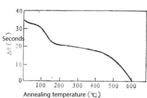
(a) the relationship between the angular distance between the main peak and subpeak and the annealing temperature; (b) the relationship between the half width of the main peak and the maximum reflection coefficient and the annealing temperature. The unimplanted samples are 4.34 seconds and 0.64 seconds, respectively.
From the backscattering of ion implantation damage, it is found that the serious damage is not on the surface of the crystal, but at a certain depth below the surface. If the energy of implanted ions is more than $1\mathrm{MeV}$, an amorphous layer is formed at a certain depth on the wafer surface, and the crystal part containing the amorphous layer becomes a strictly parallel double wafer. When taking the appearance phase diagram of this kind of wafer, just like the highly parallel double wafer, it can produce X-ray water pattern interference fringes with visible spacing. Figure 33 A group of topography of silicon wafers bombarded by 2MeV energy N + ions are given. In the picture, we can see the three regions with different contrast shown by the
symbol 1, 2, and 3, which is the result of the inhomogeneity of the ion beam. Region 1 is the unimplanted area blocked by the mask, and area 2 is the area under bombardment. Region 3 is bombarded with the highest ion density, that is, the highest dose, and obvious stripes patterns can be seen. When the Mo target is replaced by the Cu target, the reflection fringe density is higher (see figure 33 (a) the illustration on the upper right.
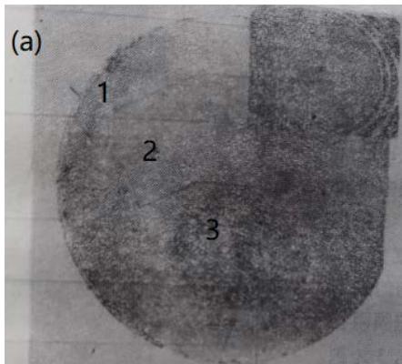 Fig. 31: The derivation of the relation of $\Delta \theta_{\mathrm{i}} = 2\delta_{\mathrm{i}}$ bending Wafer.
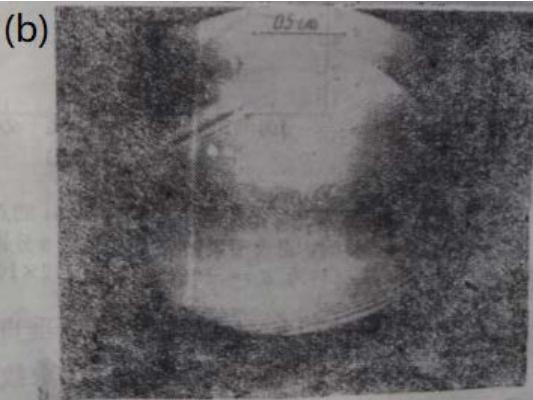 Fig. 33: X-ray topography of $2\mathrm{MeV}$ $\mathsf{N}^+$ ion bombardment wafer [27]. Area 1 is blocked by mask, area 2 is bombarded. (a) Mo target, 11-1 reflection transmission phase diagram, the upper right corner illustration shows Cu target radiation, 115 reflection corresponding to region 3; (b) Cu radiation of the same wafer, 333 reflection appearance diagram
The model of wafer damage after heavy ion bombardment is shown in figure As shown, it includes five areas, namely, the power of the injection layer. The school district, the sports district, the power district and the sports district in the bulk crystal, and the amorphous region surrounded by two sports districts. The dynamic region suffered only some minor injuries; the sports district contained varying degrees of severe damage, but remained single crystal. The volume of the amorphous region is $10\%$ larger than that of the crystalline region, so the atoms move along the boundary of the region to the un-bombarded region.
This displacement $|C|$ is schematically shown in figure 34(b) in the figure, the damage profile along the $Z$ axis is shown by the shifted atomic concentration $N_{i}$.
(C) it can be seen that the damage changes continuously in the direction of $z$ -axis, in the same area and from one area to another.
The amorphous region shows a maximum value.
Schwuttke et al have studied the change of the transmission phase diagram of the sample annealed after bombardment with this kind of high energy ion, and found that. The contrast of the bombardment-un-bombarded boundary changes obviously, indicating that the lattice expansion of the bombardment zone is relaxed and increases with the annealing temperature.
With the extension of the addition time, the lattice of the bombarded region continues to relax until it is stable, when the amorphous region is transformed into non-quasicrystals.
The lattice damage and recovery of the implanted samples are also confirmed in the study of low energy implanted samples.
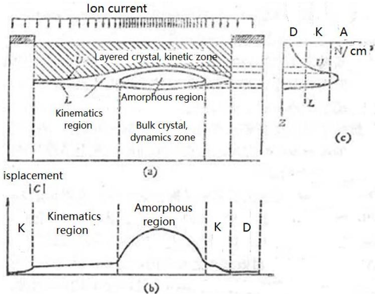 Fig. 34: Radiation damage model in silicon wafers after ion implantation.
(a) the cross section of the bombarded wafer, (b) the outline of the atomic displacement of the bombarded wafer, and (c) the degree of damage of the bombarded wafer.
D, K and A. represent separately Dynamic, Kinematics and Amorphous region
## XIII. GENERATION AND ELIMINATION OF INDUCED DISLOCATIONS
From the above, it can be seen that to avoid the generation of induced defects in order to establish a reasonable and optimal thermal process is an urgent problem for integrated device manufacturers to solve, and to study the generation and elimination of induced dislocations is for this purpose. The generation of induced dislocations is a very complex problem, which involves many technological factors. We synthesize the existing research results according to the stress-strain point of view.
### a) Introducing dislocations by internal stress
When the device is fabricated, the lattice parameters of the diffusion layer are different from the matrix, and there is a mismatch stress due to the lattice mismatch. When the internal stress reaches a certain value, the mismatch dislocation will be introduced. To parameter mismatch dislocations a minimum diffuser concentration $Q_{\mathrm{min}}$ is necessary. $Q_{\mathrm{min}}1.13\mathrm{CsDt}$ where the $C_s$, $D$, $t$ is the surface concentration, diffusion coefficient and diffusion time, respectively. For phosphorus in silicon, the lowest concentration is $C_s \approx 5 \times 10^{20} \times \mathrm{cm}^3$, while that of boron is $1 \times 10^{20} / \mathrm{cm}^3$. Dislocations are introduced beyond this concentration, and an example is shown in figure 35.
In order to overcome the introduction of dislocation caused by mismatch stress, Yeh [38] proposed a method of stress compensation, that is, when diffusing P, B, Sn is diffused at the same time. The effective method to study the diffusion stress and stress compensation is to observe the swing curve of double crystal diffraction and satellite reflection.
 Fig. 35: Shows the X-ray topographies of the dislocation introduced by the edge of the diffusion zone
Mismatch dislocations will also be introduced between the epitaxial layer and the substrate due to lattice mismatch. Sugita and Tamura [39] X-ray double crystal diffractometer using B-doped substrate $\mathsf{P - P^{+}}$ epitaxial growth found that the mismatch dislocation is also related to the resistivity of the substrate. The dislocation caused by the mismatch between the epitaxial layer and the substrate is particularly prominent in the heteroepitaxy of compound semiconductors.
### b) Introducing dislocations by external stress
The external stress that can introduce dislocations into the high temperature process of silicon integrated devices includes mechanical damage, such as heavy scratches, etching marks and gaps on the edge of the wafer, cracks, damage of the reference edge, excessive temperature gradient or thermal stress caused by rapid cooling and heating, etc.
## i. Dislocation caused by mechanical damage
At a certain temperature, if the stress of mechanical damage exceeds the yield limit of silicon single crystal at this temperature, slip dislocation will be introduced. Obviously, whether mechanical damage can produce dislocation is related to the degree of mechanical damage, the temperature of treatment and whether there is a temperature gradient. Figure 36.
In the case of the dislocation introduced by the "△" mark after 6 hours of $1200^{\circ}\mathrm{C}$ treatment, it can be seen that the lighter scratches hardly introduce dislocations, while the heavy and thick scratches produce a large number of dislocations.
Figure 37 shows the dislocation at the crack tip at the edge of the silicon wafer. This induced dislocation will also be added and extended in the following high temperature cycle. It can be seen that the mechanical damage such as edge collapse and notch at the edge of the wafer is the potential source of dislocation, so these damages should be avoided as far as possible.
## ii. Dislocation is introduced by wafer bending
Wafer bending will directly affect the alignment of lithography patterns, and dislocations will be introduced in the following high temperature cycle. Huff et al. [40] found that if there is warping of dozens of $\mu$ m caused by machining in 50mm wafers, it is sufficient to produce dislocations in $1200^{\circ}\mathrm{C}$. If the curved substrate is concave on one side of the epitaxial growth, only the center is at high temperature, so there is compressive stress, resulting in a large number of dislocations due to normal deformation near the center of the wafer [41]. If the local bending of the wafer is large enough (the radius of curvature is small enough), a large number of dislocations can be introduced due to multilateralization during annealing.
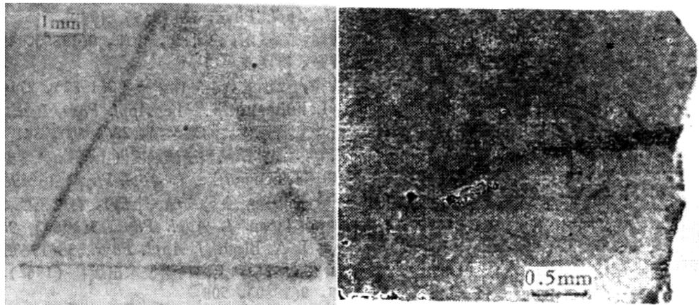 Fig. 36: Transmission topography of silicon wafer. There are Fig. 37 shows the X-ray topography scratches on the back of the wafer. After $1200^{\circ}\mathrm{C}$ annealing of edge cracks and dislocation for 6 hours, there are a large number of induced dislocations increment in silicon wafers, MoKα radiation. (2-20) reflection. MoKα radiation, (2-20) reflection
## iii. Dislocation is introduced by thermal stress
In the fabrication of silicon devices, dislocations will be introduced due to thermal stress. Figure 38 shows the phase diagram of the two wafers in 20 seconds (a) and 5 minutes (b). It can be seen that the introduction of the former from the edge of the wafer is much more serious. In order to restrain the completion of thermal stress introduction, special attention should be paid to the heating and cooling rate higher than that of 900oC. Hear et al. [42] used capped quartz boat and further improved quartz boat to achieve good results.
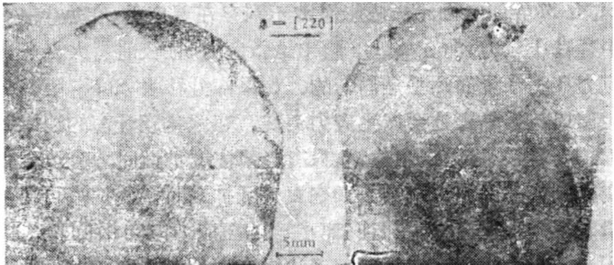 (a) Fig. 38: Effect of wafer speed on induced dislocations. (a) in and out of the furnace within 20 seconds. (b) 5 minutes into the oven and 10 minutes out of the oven
## iv. Introducing dislocations by stress abrupt change
After oxidation or nitriding, there is stress on the interface of $\mathrm{SiO}_2$ -Si, $\mathrm{Si}_3\mathrm{N}_4$ -Si due to the difference of thermal expansion coefficient. There is a compressive stress in the thermally grown $\mathrm{SiO}_2$ film and a tensile stress in the $\mathrm{Si}_3\mathrm{N}_4$ film, which is much larger than the former, and the stress is almost uniform at the whole interface. If the $\mathrm{Si}_3\mathrm{N}_4$ film is partially removed, abrupt stress changes will occur in places such as diffusion windows, cracks, etc. There is elastic distortion at the edge of the oxide film window, but it is not enough to produce dislocations. Only when there is a high concentration of diffusion will the state of the image distortion region be changed and dislocations will be introduced. For example, when diffusing in the emitter region, phosphorus diffusion can produce compressive stress near the edge of the window, and the compressive stress direction of the $\mathrm{SiO}_2$ film is the same. The stress mutation caused by this strain can produce dislocations at the edge of the diffusion window, which is called emitter edge (EE) dislocation. This EE dislocation has an obvious effect on the gain $\beta$ of the device. Schwuttke and Fairfield [43] have observed that dislocations occur under the edge of the oxide window after boron diffusion and extend from the diffusion zone to the non-diffusion zone. As shown in figure 35.
## XIV. THE SUMMARY
The above 13 sections are the contents and results of modern test analysis and research of silicon materials in integrated device engineering. Let's sum it up.
integrated circuits or ultra-large-scale integrated circuits, single crystals with $< 111>$ or $< 100>$ orientation are required. Single crystals with this orientation must be prepared by Czochralski or floating zone method. The process of growing this oriented silicon single crystal is complex and fastidious. The process and crystal defects are discussed in sections 3 and 4. But the question of resistivity is involved.
Most of the high-purity polysilicon materials are neutral and fail to reflect N-type or P-type. However, single crystals must be N-type or P-type, and require a certain resistivity. It is necessary to doping the fused polysilicon (N-type or P-type) when preparing the single crystal, and control the doping concentration to make the finished single crystal achieve the required resistivity.
### (3) The preparation stage of the wafer
In the development (production) unit of integrated devices, the required silicon single crystals are generally segments, and the silicon single crystals grown by Czochralski and floating zone methods are cylindrical in shape. The growth edges of the cylinder surface are symmetrically distributed three times (\<111> orientation) and four times (\<100> orientation).
#### Preparation of rolling circle and reference plane
Previously, the circle has been discarded, because the circle will cause damage to the crystal surface. Cutting the wafer with this round crystal will inevitably leave damage around the wafer, and this mechanical damage will become the source of slip dislocation in the subsequent thermal process. Now the first step is to make the reference plane (edge). For $<100>$ oriented crystals, the reference plane should be parallel to the line of diagonal growth edges, while for $<111>$ oriented crystals, the reference plane should be parallel to the line of two growth edges. It is generally prepared by mechanical grinding. It is worth noting that after the reference surface is prepared, chemical methods are used to corrode the grinding surface to minimize mechanical damage.
#### > Directional cutting
Generally, optical orientations are used to observe the appearance of third (or fourth) symmetrical reflectors.
Fine adjustment of the crystal is the best image symmetry, which can be mechanically cut, so that it can meet the process requirements in general. However, for the $\{111\}$ wafers to be epitaxially grown, the accurate $\{111\}$ is not needed, which causes a deviation of $2\sim 4^{\circ}$ degrees from the nearest $< 110>$. At this time, after obtaining the best cubic symmetrical light emission image, if the spot is directly above the observation screen, the crystal should be tilted upward by $2\sim 4^{\circ}$ degrees; if the best cubic symmetrical spot is directly below the observation screen, it should be bent down by $2\sim 4^{\circ}$ degrees. There's nothing wrong with it.
#### > Grinding and polishing of wafers
Generally, it should be ground on both sides, preferably mechanochemical grinding, to reduce cutting damage. One-sided mechanochemical polishing can not only meet the requirements of wafer surface flatness and finish, but also minimize grinding damage.
#### (4) Enter the thermal process
- The first thermal process is generally oxidation. It is suggested that wet oxygen oxidation should not be carried out directly, but should be annealed for 30 minutes and then with wet oxygen in order to reduce the occurrence of oxidation stacking faults. Similarly, if the first thermal process is epitaxial, the wafer should be annealed for a certain period of time before epitaxial growth, in order to reduce epitaxial growth stacking faults.
- In the first lithography, it is necessary to pay special attention to the long edge of the chip diagram and the reference edge of the chip, so as to ensure the highest yield at the end of the chip.
#### (5) The best thermal process
In this chapter, we spend a lot of space to study the law of induced defects, and we know that they are all related to the mechanical damage and thermal process around the surface of the wafer. Therefore, it is summarized as "the best hot process":
- In the process of wafer preparation, such as the preparation, cutting, grinding and polishing of the reference surface, we should try our best to reduce the mechanical damage around and on the surface of the wafer.
- > In and out of the high temperature furnace must be slow to reduce the thermal stress caused by thermal shock. Never fast in and out.
- The quartz boat where the wafer is placed must be flat, and the wafer cannot be placed vertically or tilted to avoid bending or warping of the wafer at high temperature. It is best to put a lid on the quartz boat after placing the chip.
#### (6) Chip segmentation
Because the cleavage plane of the silicon crystal is $\{111\}$, there are strict requirements for the arrangement of the chip pattern, so a reference edge is made on the wafer, which is the intersection of the inclined $\{111\}$ plane and the wafer surface. Therefore, the long edge of the chip pattern should be parallel to the reference edge. After the completion of the planar process of chip fabrication, the process of chip segmentation should be carried out sequentially. For the $\{100\}$ wafer, as long as the direction of the blade is parallel to the reference edge, both directions can be split along the cleavage plane, while for the $\{111\}$ wafer, the first knife must be parallel to the reference edge, and after the scribing in this direction is completed, then make a vertical scribing. The direction of rolling the wafer must be perpendicular to the reference edge so that the chip can split along the $\{111\}$ cleavage plane, but the direction perpendicular to the reference edge is not split.
Generating HTML Viewer...
References
43 Cites in Article
Xu Shunsheng,Yang Chuanzheng (1980). X-ray appearance observation and analysis of crystal defects.
Yang Chuanzheng (1978). Silicon Germanium Device Application Market Overview.
Yang Chuanzheng,Xu Jingyang (1987). applications in semiconductor crystal and device technology.
Yang Chuanzheng,Tian Peilan (1978). Device Operation as Crystal Quality Probe.
H Sandmann (1969). CHEM SERVICE, INC..
Si Chongkui,Yang Huang Zhaobin,Chuanzheng (1982). Vapor Silicon single Crystal growth.
Yang Chuanzheng (1982). growth Edge formation and Polar Graph Analysis of Silicon single crystals.
Yang Chuanzheng,Xu Shunsheng (1977). growth edges of Cylindrical Silicon single crystals.
Yang Chuanzheng,Xu Shunsheng (1981). X-ray topography observation of several phenomena in the growth of dislocation-free silicon single crystals.
Yang Chuanzheng,Zhu Jiansheng (1982). Research on defects in Zone fused Silicon single Crystal in hydrogen and Argon atmosphere.
Cui Shufan,Mai Zhenhong (1983). Electronic structures and the properties of hydrogen in silicon.
Cui Shufan,Ge Peiwen,Wu Zhao Yaqin,Lansheng (1979). existence and influence of Si-H Bond in Silicon single Crystal.
Jiang Berlin,Sheng Shixiong,Xiao Zhigang (1980). formation mechanism of defects in zone fused silicon single crystal heat treatment in hydrogen atmosphere.
Chen Yansheng,Liu Guirong,Li Huaixiang (1996). Elimination and Application of hydrogen-induced defects and Micro-defects hydrogen precipitation in Silicon.
Cui Mak Zhenhong,Fu Shufan,Quangui (1984). X-ray morphology observation of primary microdefects in undecorated Czochralski silicon.
Duan Pei,Ping Gao (1987). study on primary vortex defects in Czochralski silicon.
Li Zongquan,Shen Hui,Qin Yong (1991). observation of primary microdefects in Czochralski silicon.
Bao Ximao,Ji Fuquan,Huang Xinfan (1982). study of oxide faults in the surface layer of silicon wafers with deviation from < 111 > orientation.
C Drun,C Clark (1968). Unknown Title.
K Bean,P Gleim (1968). The influence of crystal orientation on silicon semiconductor processing.
Chen Mingqi,Yang Chuanzheng,Wang Guangfu (1982). study on Epitaxial pattern distortion of Silicon (111) Wafers.
Yang Chuanzheng (1977). the Best orientation of Silicon Wafer.
J Fairfield,G Schwuttke (1966). The Influence of Crystallographic Defects on Device Performance.
A Authier,D Simon,A Senes (1972). Correlation between lattice defects and electrical properties of silicon Zener diodes.
E Jungbluth,P Wang (1966). Structural Defects and Junction Characteristics in Silicon Transistors.
G Schwuttke (1970). Silicon material problems in semiconductor device technology.
G Schwuttke,K Brack,E Hearn (1971). The influence of stacking faults on leakage currents of FET devices.
Seigo Kishno,Atsuko Noda (1972). Observation of Lattice Defects in Ion-Implanted Si Wafer by A Double Crystals Spectrometer Method.
D Lecrosnier,G Pelous,J Burgeat (1977). Investigation of ion-implantation damage with x-ray double reflection.
G Schwuttke,K Brack (1969). Unknown Title.
G Schwuttke,K Brack,E Gorey,A Kahan,L Lowe,F Euler (1972). Formation and annealing of isolation regions in silicon through Si+ bombardment.
No ethics committee approval was required for this article type.
Data Availability
Not applicable for this article.
How to Cite This Article
Chuan-Zheng Yang. 2026. \u201cTest and Research of Silicon Materials in Integrated device Engineering\u201d. Global Journal of Science Frontier Research - A: Physics & Space Science GJSFR-A Volume 23 (GJSFR Volume 23 Issue A4): .
Explore published articles in an immersive Augmented Reality environment. Our platform converts research papers into interactive 3D books, allowing readers to view and interact with content using AR and VR compatible devices.
Your published article is automatically converted into a realistic 3D book. Flip through pages and read research papers in a more engaging and interactive format.
It is of great practical significance to test and analyze the quality of silicon materials used in integrated devices and their changes in planar thermal process. This paper summarizes the international test, analysis and research results. The contents include polycrystal preparation, single crystal growth and its crystal defects, wafer cutting, grinding and polishing, wafer tracking observation and analysis in plane thermal process, generation control and elimination of induced dislocations, etc.
Our website is actively being updated, and changes may occur frequently. Please clear your browser cache if needed. For feedback or error reporting, please email [email protected]
Thank you for connecting with us. We will respond to you shortly.