Measured resistivities of produced silicide showed their good conductive properties. The calculation of technological route for obtaining thin silicide contacts (
## I. INTRODUCTION
In a metal-semiconductor contact, depending on the ratio between the values of the electron yield work in the metal $\psi_{\mathrm{m}}$ and in the semiconductor $\chi + V_{\mathrm{n}}$, electrons as a result of internal emission may pass from metal to semiconductor or vice versa. In this case, a part of electrons from the metal (silicide) goes to the semiconductor (Si) until thermodynamic equilibrium occurs and the Fermi levels in the metal and in the semiconductor are equalized [1,2].
In the vicinity of the semiconductor-metal interface in the semiconductor an area of depleted charge carriers arises, an area of bulk charge of uncompensated negative acceptor ions whose electric field prevents the further emission of electrons from metal to semiconductor, the semiconductor energy bands bend downwards.
If the thickness of the intermediate layer is atomic distance, then the magnitude of the curvature of the height of the potential barrier equals the contact potential difference
$$
\psi_ {m S} = \Phi_ {S} - \Phi_ {m} + \left(E _ {f} - E _ {\nu}\right) = X + E _ {g} - \Phi_ {m},
$$
where, the second term is the difference between the yield work of the metal and the electron affinity of the semiconductor.
Under the influence of IR radiation two types of electronic transitions can take place in such a structure. If the incident photon energy $\mathrm{hv} \geq \mathrm{E}_{\mathrm{g}}$, then electron-hole pair generation occurs when it is absorbed in the semiconductor. In this case, as well as in an ordinary photodiode on a p-n junction, carriers of different sign on the junction field separate and photo-electric power arises. It is obvious that the long-wave limit of such a process cannot be less than the band gap width of the semiconductor, and from this point of view the Schottky barrier photodiodes do not differ from p-n photodiodes or their own photoresistors. If $\mathrm{hv} < \mathrm{E}_{\mathrm{g}}$ then infrared absorption in a metal film excites valence electrons to states above the Fermi level, leading to holes, some of which have energy greater than the barrier height $\Psi_{\mathrm{ms}}$. Then either the hole is emitted from the metal to the semiconductor, or the electron moves from the semiconductor to the metal, filling the empty state [3,4]. To overcome the metal-to-semiconductor barrier, the energy of the excited hole must be greater than the height of the barrier. The long-wave boundary of such a process can be changed by selecting the appropriate metal. Therefore, from the point of view of creating silicon-based IR photodetectors the greatest interest is the photoemission from metal to semiconductor.
### a) Experiment
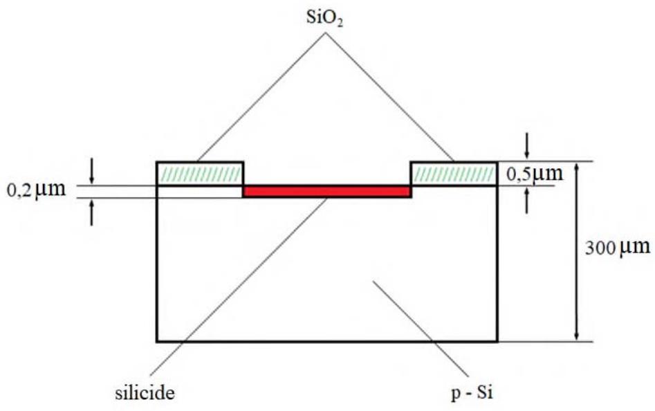
In the first step, the $0.5\mu \mathrm{m}$ thick $\mathrm{SiO}_2$ oxide layer was grown on p-type (100) silicon wafers (KDB-10). Before this operation the silicon wafers were degreased with trichloroethane, acetone and alcohol and cleaned in a $\mathrm{CCl}_4$ boiling solution. Before metal (Ni) sputtering, windows of $2.2\mathrm{mm}$ and $4.4\mathrm{mm}$ were opened in the $\mathrm{SiO}_2$ film using photolithography techniques. Metal sputtering was carried out thermally in a vacuum of $10^{-5}\mathrm{mmHg}$. The substrate temperature was maintained at $200^{\circ}\mathrm{C}$. Immediately before loading into the vacuum chamber Si wafers were pickled by buffer solution of HF ( $34.6\% \mathrm{NH}_4\mathrm{F} + 6.8\% \mathrm{HF} + 58.6\% \mathrm{H}_2\mathrm{O}$ ) with the following washing of wafers in deionized water and drying in isopropyl alcohol vapor. After metal deposition the silicon wafers were annealed at $\mathrm{T}_{\mathrm{ann}} = 510^{\circ}\mathrm{C}$ and $\mathrm{T}_{\mathrm{ann}} = 900^{\circ}\mathrm{C}$ for $\mathrm{t} = 30$ min in $\mathrm{N}_2$ atmosphere to obtain NiSi - Si and $\mathrm{NiSi}_2$ - Si structures.
Fig. 1 shows the cross-section of the investigated structures. Photoconductivity spectra of the obtained NiSi - Si and $\mathrm{NiSi}_2$ -Si structures with the Schottky barrier were studied.
 Figure 1: Cross Section of Nickel Silicon-Silicide NiSi - Si Structure
## II. DISCUSSION OF RESULTS
Figures 2 and 3 show the V- I characteristics of the NiSi - Si and $\mathrm{NiSi}_2$ - Si structures, and figures 3 and 4 show the inverse V- I characteristics of the NiSi - Si structures in the absence of incident radiation. 3 and 4
the inverse V- I characteristics of NiSi - Si structures in the absence and presence of incident radiation. Figures 2 and 3 show that the V- I characteristics of NiSi - p - Si and $\mathrm{NiSi}_2$ - p - Si structures at room temperature are very different.
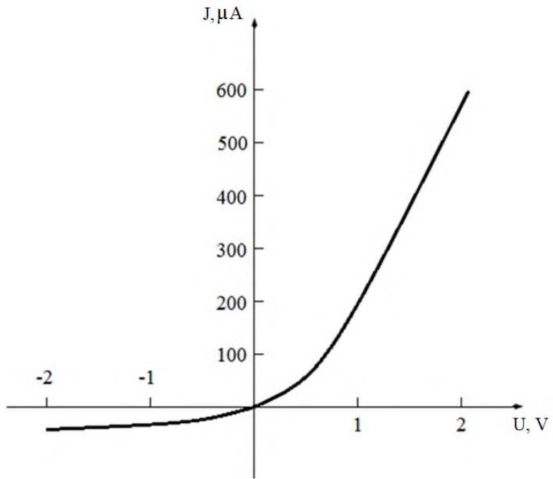 Fig. 2: The V- I Characteristic of NiSi - p - Si Structure at T = 300 K
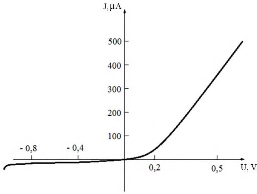 Fig. 3: The V- I Characteristic of $\mathrm{NiSi}_2$ - p - Si Structure at $T = 300\mathrm{K}$
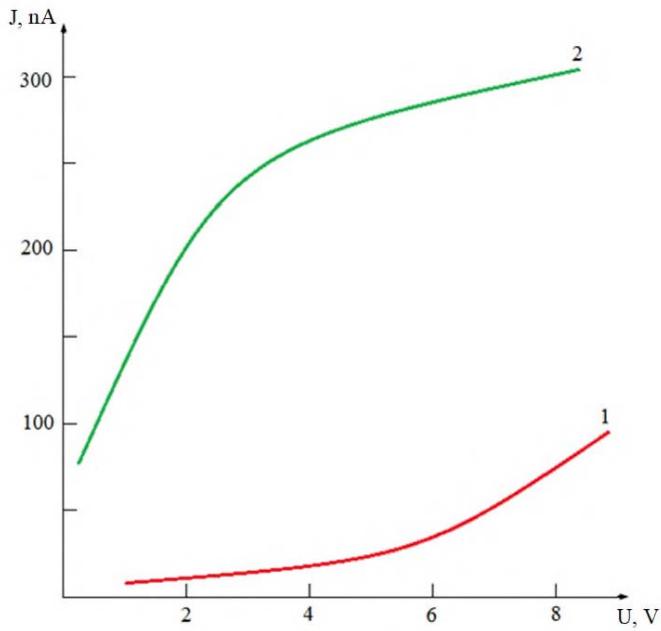 Fig. 4: Inverse V-I Characteristics of NiSi - p - Si Structure: 1 - in Absence of Illumination, 2 - with Light Illumination $\lambda = 2\mu m$
Inverse currents differ by more than an order of magnitude and it was found that for the $\mathrm{NiSi}_2 - p - Si$ structures the V- I characteristic does not change its appearance up to frequencies of $100\mathrm{kHz}$, but for the NiSi - p - Si structures at frequencies above 1 kHz strong distortions of the V- I characteristic are observed. A spectrophotometer IKS-14A tuned to a wavelength $\lambda = 2\mu \mathrm{m}$ was used as a light source. The light hits the silicide from the Si side (back illumination).
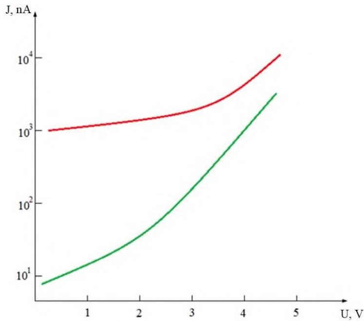 Fig. 5: Inverse V- I Characteristicsof $\mathrm{NiSi}_2$ - p - Si Structure: 1 - in Absence of Illumination, 2 - with Light Illumination $\lambda = 2\mu m$
As can be seen from fig. 4 and 5 a considerable change of a current through the investigated structures at illumination is observed: the current through the investigated structures at illumination increases in 100 - 200 times at small values of the applied reverse voltage $(V_{R} = 200 - 800\mathrm{mV})$, in 10 - 50 times at higher reverse biases $(V_{R} = 1 - 2\mathrm{V})$; at voltages 4 - 6 V a current change makes only 1,1 - 5 times, i.e. the best mode of structures with the Schottky barrierNiSi - p - Si $V_{\mathrm{R}} = 1 - 2$ V. At higher voltages the leakage currents increase and also breakdown of investigated samples occurs. For structures NiSi - p - Si and $\mathrm{NiSi}_2$ a considerable change of current at illumination at wavelength $\lambda = 2\mu \mathrm{m}$ at various values of applied reverse bias ( $V_{\mathrm{R}} = 0,1 - 5\mathrm{~V}$ ) was observed.
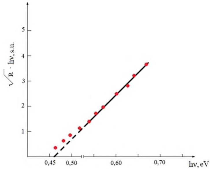 Fig. 6: Dependence of $R^{1/2} \cdot hv$ Value on Barrier Height for NiSi - p - Si Structures: $T = 80 \, \text{K}$; $V_R = 154 \, \text{mV}$
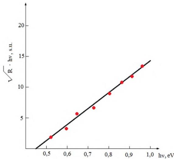 Fig. 7: Dependence of $R^{1/2} \cdot hv$ Value on Barrier Height for NiSi - p - Si Structures: $T = 80 \, \text{K}$; $V_R = 380 \, \text{mV}$
The experimental results for photosensitivity are in accordance with the refined Fowler formula [5]. These data were used to determine the Schottky barrier height. Figures 6, 7 and 8 the dependences $R^{1/2} \cdot hv$ on the incident photon energy hv are plotted. The point of intersection with the energy axis gives the barrier height, which is for NiSi - Si structures $\Psi_{\mathrm{ms}} = 0.46\mathrm{eV}$.
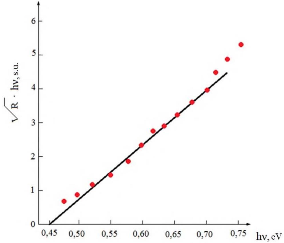 Fig. 8: Dependence of $R^{1/2} \cdot hv$ Value on Barrier Height for NiSi - p - Si Structures: $T = 80 \, \text{K}$; $V_{R} = 0 \, \text{mV}$
Figures 9, 10 and 11 show experimental dependences of sensitivity of structures PdSi - p - Si, Pt $_2$ Si - p - Si and PtSi - p - Si at temperature $T = 77(80 \mathrm{~K})$ at constant incident radiation power. The measurements were made on a spectrophotometer IKS-31 (temperature of the global bar $T = 500^{\circ} \mathrm{C}$ ).
Samples PdSi - p - Si and PtSi - p - Si were made according to previously described technique. Figures 9, 10 and 11 show that the wavelength dependence of photosensitivity is approximately described by Fowler formula.
The Schottky barrier height determined from the photoelectric measurements obtained from the dependence $R^{1/2} \cdot h\nu = f(h\nu)$ was $\Psi_{\mathrm{ms}} = 0.38 \, \mathrm{eV}$ for PdSi - p - Si and $\Psi_{\mathrm{ms}} = 0.26 \, \mathrm{eV}$ for PtSi - p - Si (fig. 11). The values of the Schottky barrier heights obtained in this way were also confirmed by photoelectric measurements. A study of the annealing temperature dependence for the PtSi - p - Si and PtSi - n - Si structures has shown that $\varphi_{8}$ for the first type structure weakly depends on the annealing temperature, while for the second type structure this dependence passes through a maximum. The latter character of the dependence has found its explanation in the multicontact theory [6,7].
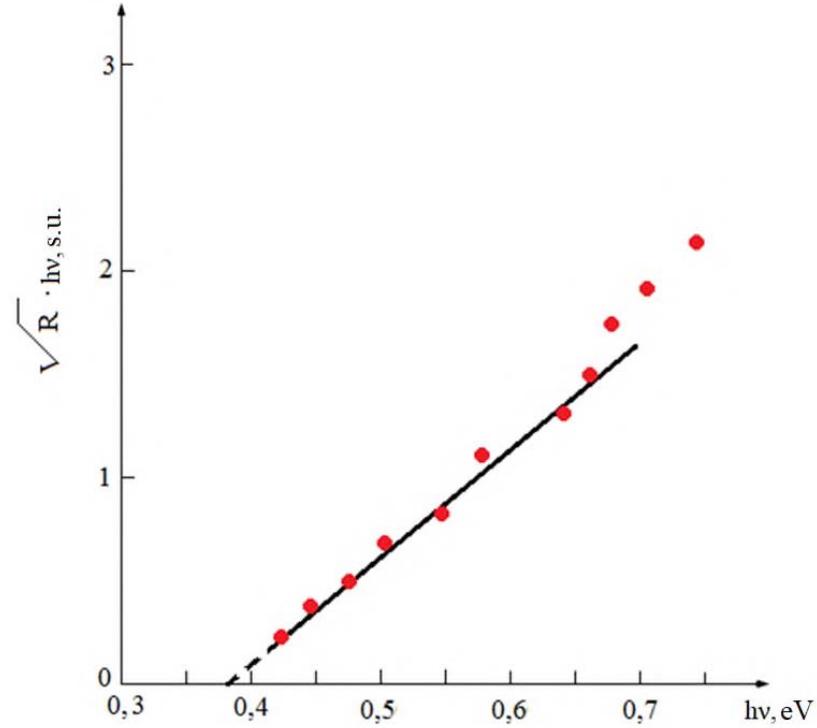
 Fig. 9: Dependence of $\mathrm{R}^{1/2}$ -hv Value on Incident Photon Energy for PdSi - p - Si Structure at T = 770 K Figure 10: Spectral Dependence of Sensitivity of $\mathrm{Pt}_2\mathrm{Si}$ - p - Si Structure at T = 80 K
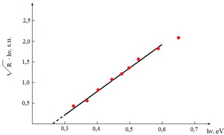 Fig. 11: Dependence of $\mathsf{R}^{1 / 2}$ -hv Value on Energy of Incident Photons for PtSi - p - Si Structure at T = 80 K
It is shown that the direct currents of these structures are proportional to their active area. It is found that all characteristic parameters of contacts made on Si substrate (111) are somewhat lower than those of contacts made on Si substrate (100).
## III. CONCLUSION
It is found that the sensitivity of the NiSi - p - Si structure is significantly higher than that of the $\mathrm{NiSi}_2$ - p - Si structures. In addition, an increase in sensitivity with decreasing nickel silicide thickness was observed. The optimum mode of operation of the NiSi - p - Si structure and its photosensitivity at a wavelength of $2\mu \mathrm{m}$, which was $R = 0,05 - 0,1\mathrm{mA} / \mathrm{W}$, were determined.
Generating HTML Viewer...
References
7 Cites in Article
V Brudnyĭ,N Kolin,L Smirnov (2007). The model of self-compensation and pinning of the Fermi level in irradiated semiconductors.
M Shapochkin (2004). Statisticheskaya fizika / M. B. Shapochkin.
V Qoldade,L Pinchuk (2009). Fizika kondensirovannoqo sostoyaniya.
A Zakharov (2006). Fizicheskiye osnovi mikroelektroniki: ucheb.
V Frolov,; Frolov,S Pimenov,V Konov,E (2008). Razmerniy effekt v rabote vixoda elektronov / V.D.
Ya,Ya,V Kudrik,V Shinkarenko,R Slepokurov,R Biqun,Ya,Kudrik (2014). Metodi opredeleniya visoti baryera Shottki iz volt-ampernikh kharakteristik// Optoelektronika i poluprovodnikovaya tekhinka.
V Shashkin,A Murel,V Danilchev,O Khrikin (2002). Upravleniye kharakterom tokoperenosa v baryere Shottki s pomoshyu δ-leqirovaniya: raschet I eksperiment dlya Al/GaAs.
No ethics committee approval was required for this article type.
Data Availability
Not applicable for this article.
How to Cite This Article
E.A. Kerimov. 2026. \u201cPhotosensitive Structure with Schottky Barrier Based on Nickel-Silicon Silicon Contact\u201d. Global Journal of Research in Engineering - G: Industrial Engineering GJRE-G Volume 23 (GJRE Volume 23 Issue G2): .
Explore published articles in an immersive Augmented Reality environment. Our platform converts research papers into interactive 3D books, allowing readers to view and interact with content using AR and VR compatible devices.
Your published article is automatically converted into a realistic 3D book. Flip through pages and read research papers in a more engaging and interactive format.
Measured resistivities of produced silicide showed their good conductive properties. The calculation of technological route for obtaining thin silicide contacts (
Our website is actively being updated, and changes may occur frequently. Please clear your browser cache if needed. For feedback or error reporting, please email [email protected]
Thank you for connecting with us. We will respond to you shortly.