
Loading menu…

Study of Two-layer System TiN / Ni 0.905 W 0.095 Adoptable for Creating Paramagnetic Substrates with Cubic Texture for 2G HTS Superconductors

Study of Two-layer System  TiN / Ni 0.905 W 0.095 Adoptable for Creating Paramagnetic Substrates with Cubic Texture  for 2G HTS Superconductors

Article Fingerprint

ReserarchID

SFRZ56PN

Study of Two-layer System  TiN / Ni 0.905 W 0.095 Adoptable for Creating Paramagnetic Substrates with Cubic Texture  for 2G HTS Superconductors Banner

Key Research Insights

Synthesized scholarly intelligence & interactive research assistant
  • English
  • Afrikaans
  • Albanian
  • Amharic
  • Arabic
  • Armenian
  • Azerbaijani
  • Basque
  • Belarusian
  • Bengali
  • Bosnian
  • Bulgarian
  • Catalan
  • Cebuano
  • Chichewa
  • Chinese (Simplified)
  • Chinese (Traditional)
  • Corsican
  • Croatian
  • Czech
  • Danish
  • Dutch
  • Esperanto
  • Estonian
  • Filipino
  • Finnish
  • French
  • Frisian
  • Galician
  • Georgian
  • German
  • Greek
  • Gujarati
  • Haitian Creole
  • Hausa
  • Hawaiian
  • Hebrew
  • Hindi
  • Hmong
  • Hungarian
  • Icelandic
  • Igbo
  • Indonesian
  • Irish
  • Italian
  • Japanese
  • Javanese
  • Kannada
  • Kazakh
  • Khmer
  • Korean
  • Kurdish (Kurmanji)
  • Kyrgyz
  • Lao
  • Latin
  • Latvian
  • Lithuanian
  • Luxembourgish
  • Macedonian
  • Malagasy
  • Malay
  • Malayalam
  • Maltese
  • Maori
  • Marathi
  • Mongolian
  • Myanmar (Burmese)
  • Nepali
  • Norwegian
  • Pashto
  • Persian
  • Polish
  • Portuguese
  • Punjabi
  • Romanian
  • Russian
  • Samoan
  • Scots Gaelic
  • Serbian
  • Sesotho
  • Shona
  • Sindhi
  • Sinhala
  • Slovak
  • Slovenian
  • Somali
  • Spanish
  • Sundanese
  • Swahili
  • Swedish
  • Tajik
  • Tamil
  • Telugu
  • Thai
  • Turkish
  • Ukrainian
  • Urdu
  • Uzbek
  • Vietnamese
  • Welsh
  • Xhosa
  • Yiddish
  • Yoruba
  • Zulu
Reading Preferences
Font Size
Line Spacing
Background
This converted HTML version may contain rendering inconsistencies. Please refer to the PDF for the authoritative version, or click here to provide feedback.

Abstract

The influence of deposition conditions on the morphology and structure of the two-layer system TiN / Ni 0.905 W 0.095 were studied. The effect of concurrent formation of cube texture both in substrate based on paramagnetic alloy Ni 0.905 W 0.095 and TiN coating was detected by means of xray diffraction analysis. Composition TiN / Ni 0.905 W 0.095 may be used as a substrate in the conductive architecture of 2G HTS to improve its critical current density.

I. INTRODUCTION

Research in the field of high-temperature superconductors of the second generation (2G HTS) based on YBCO textured films is of particular interest because it opens up new perspectives for creating coated conductors, which could operate in high magnetic fields at temperature of liquid nitrogen (77.4 K). [1 – 6]. First off all this refers to the transfer of electric current over long distances (in particular from the NPP to the consumer), the creation of powerful magnetic fields, etc [7, 8]. As known the architecture of 2G HTS [9] with crucial current density above jc∼106 A/cm 2 at liquid nitrogen temperature should consist of three main components [10 – 13]:

  1. Metallic substrate (thin flexible tape mostly of Ni – W alloys with different compositions);

  2. Buffer layer/layers (oxides, nitrides, in particular TiN as seed layer);

  3. Quasi monocrystalline film of high temperature superconductor YBa2Cu3O7−δ (Tc ~ 92 K [14]) with strongly reduced fraction of high angle grain boundaries.

Fabrication of high- jc, biaxially aligned HTS films can be achieved due to epitaxial growth on rolling-assisted biaxially-textured substrates (RABiTS) [11, 15 - 18]. The texture (100)[100] of the metallic substrate is conferred to the superconductor by deposition of intermediate layers which serve as a chemical and a structural buffers [19]. The presence of a conductive layer acting as an electric shunt to prevent the effect of thermal destruction of superconductor in the case of over-current opens up prospects for use of titanium nitride as the main seed buffer layer in the complex architecture of 2G HTS [20 — 22].

Moreover metallic substrate must be in paramagnetic state at low temperatures to reduce losses during ac current transport [23 - 25]. The property of paramagnetism is provided by increasing the concentration of tungsten in the Ni(1−x)Wx alloy to x∼0.095 [26, 27]. However, it hinders the formation of cube texture (100)[100] due to decreasing of stacking fault energy Es of cold-rolled alloy. The Esf decreases with increasing the content of alloying element in the alloy [28].

The main aim of this work is to find new ways to control properties of paramagnetic substrates based on Ni0.905W0.095 alloy for the creating of high-temperature superconductors with high current-carrying capacity (2G HTS).

The following research program was implemented:

  1. Experimental study of the effect of nitrogen pressure during titanium evaporation on the structural features of both components of the two-layer system TiN/Ni 0.905 W 0.095.

  2. Experimental study of the influence of TiN deposition time on the structural features of the components of the TiN / Ni0.905W0.095 system at the optimal value of nitrogen pressure.

  3. Experimental study of the influence of TiN deposition geometry on the structural features of both components of the TiN/Ni 0.905 W 0.095 system.

Development of new ways to control the structure and properties of materials based on paramagnetic Ni-W alloys with TiN coating.

II. MATERIALS AND METHODS

Preparation of substrates was carried out according to the scheme which includes following steps [29, 30]: 1) synthesis of paramagnetic alloy Ni0.905W0.095; 2) thin-layer tape production; 3) high-temperature treatment of NiW tapes; 4) deposition of titanium nitride on the surface of NiW tape; 5) XRD analysis of obtained samples.

The initial materials for obtaining the Ni – W alloys were Ni and W powders with 99.98 – 99.99% purity (by metallic impurities). The following methods were used for the purification from gaseous impurities (the main impurity is oxygen represented as nickel and tungsten oxides): 1) the heat treatment at temperatures ∼850∘C for purification of Ni powder; 2) for the refinement of W powder was applied the high-temperature treatment (1000 – 1200°C) in reducing Ar + 4% H2 gaseous mixture flow. The paramagnetic alloy was synthesized by means of powder metallurgy in deep vacuum ( p∼10−6 Torr) at T = 1200°C during t = 4 hours.

Obtained ingots were rolled up to 50 – 100 μ m at room temperatures to perform metallic tapes. The total degree of cold-rolling deformation was about 95%. The resulting operation during the tape production was high-temperature annealing at T = 1150°C during t = 2 hours.

Thin layers of titanium nitride (TiN) on the surface of Ni - 9.5 at% W tapes were obtained by the method of ion-plasma deposition[31]. Specific parameters of the TiN buffer layer deposition varied within the following ranges: negative substrate potential U = 50 - 300 V; arc current I = 80 A; temperature of substrate ts∼450∘C; nitrogen pressure in chamber pN=1.2−6.2⋅10−2Torr; deposition time τTiN=0−900s.

XRD analysis (Cu Kα radiation) was carried out to solve the following tasks: determination of the phase composition of the system components both the substrate Ni 0.905 W 0.095 and coating TiN; determination of lattice parameters; analysis of the texture of the substrate and the coating [31]; determination of the TiN coating thickness [32-34].

The method of determination the Tin-layer thickness is based on X-ray absorption. The intensity of the beam reflected from crystal plane (h k l) of a sample with the coating thickness h is as follows:

Ihkl(h)=Ihkl(0)⋅exp⁡(−2h⋅μTiN/cos⁡(θ))

Ihkl (h) – the intensity of the beam reflected from the substrate with coating;

Ihkl (0) – the intensity of the beam reflected from the substrate without coating;

h – coating layer thickness;

μTiN – the linear absorption coefficient of the coating material;

θ – the Bragg angle.

Equation (1) and mathematical modeling of the relative intensity of some X-ray interferences, in our case - the cubic plane (h 0 0) of the Ni - W substrate, makes it possible to determine the coating thickness hTIN within accuracy of about 10%.

III. RESULTS

In the present study the TiN coating was deposited on the front ("face") and the back ("shadow") side i. e out of line of sight of the cathode beam of the Ni0.905W0.095 substrates. Two series of experiments were carried out:

  • TiN deposition at constant time tTiN=3 min in a wide range of pressures of nitrogen pN=1.2−6.2⋅10−2 Torr.

  • The deposition of TiN at constant (optimal) N2 pressure of nitrogen at different times τTiN=1−3 min.

Fig. 1 and Fig. 2 present a set of diffraction patterns of the system TiN/Ni0.905W0.095 for the experimental series at different pressures for both face and shadow deposition geometries. There are two systems of diffraction lines, which belong to the FCC lattice of Ni0.905W0.095 alloy and TiN lattice of type NaCl. As the pressure of nitrogen growths, textures of the substrate and coating exhibit variations.
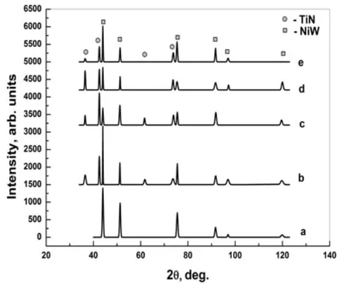
Fig. 1: Set of diffraction patterns of the system TiN/Ni
_{0.905} W _{0.095} for the experimental series at different pressures ("Shadow"): a) 0; b) 1.2, c) 1.8, d) 2.8, e) 3.8 ·10 ^{-2} Torr.
Fig. 1: Set of diffraction patterns of the system TiN/Ni 0.905 W 0.095 for the experimental series at different pressures ("Shadow"): a) 0; b) 1.2, c) 1.8, d) 2.8, e) 3.8 ·10 −2 Torr.

It is natural that the increase in pN leads to growth of the intensity of the diffraction lines of TiN, but at the same time there is a tendency to redistribute the intensities of the diffraction lines in the subsystem of Ni0.905W0.095
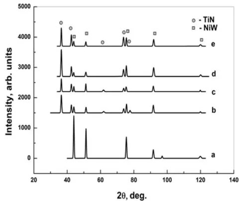
Fig. 2: Set of diffraction patterns of the system TiN/Ni
_{0.905} W _{0.095} for the experimental series at different pressures ("face"): a) 0; b) 1.2, c) 1.8, d) 2.8, e) 3.8 × 10 ^{-2} Torr.
Fig. 2: Set of diffraction patterns of the system TiN/Ni 0.905 W 0.095 for the experimental series at different pressures ("face"): a) 0; b) 1.2, c) 1.8, d) 2.8, e) 3.8 × 10 −2 Torr.

The Fig. 3 clearly shows considerable growth of intensity from Ni-W "cubic" plane I(200) at pN∼1.8⋅10−2 Torr, indicating the sharpening of cube texture of metallic component. The ratio of the cubic I(200) and diagonal I(220) diffraction lines intensity was chosen as a "texture parameter".
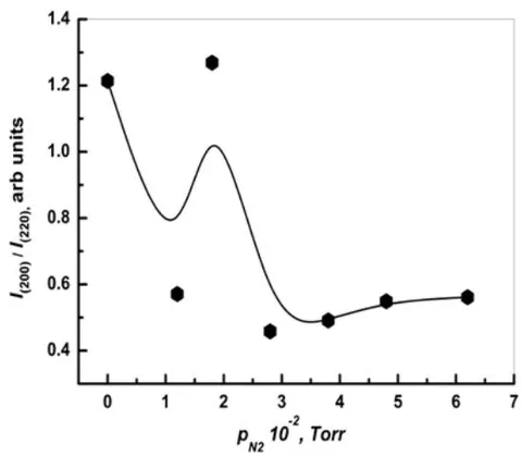
Fig. 3: Values of the ratio
I_{(200)} / I_{(220)} of the Ni_{0.905}W_{0.095} substrate after TiN deposition
Fig. 3: Values of the ratio I(200)/I(220) of the Ni0.905W0.095 substrate after TiN deposition

The Fig. 4 shows dependences of TiN lattice constant aTiN on the pressure of N2 for different coating deposition geometries.
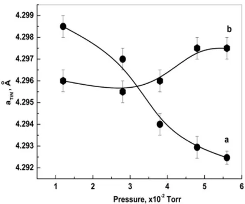
Fig. 4: The lattice parameters change of the TiN coating deposited onto the both sides of the
Ni_{0.905}W_{0.095} substrate at different pressures of nitrogen depending on the coating geometry: a) face; b) shadow.
Fig. 4: The lattice parameters change of the TiN coating deposited onto the both sides of the Ni0.905W0.095 substrate at different pressures of nitrogen depending on the coating geometry: a) face; b) shadow.

As can be seen, in the case of "shadow" geometry, the curve a is weakly dependent on the pN, while for "face" curve b decreases monotonically in the whole range of nitrogen pressures. Dynamics of variation of the TiN lattice parameter during crystalline phase formation in the coating can be associated with the change in the flux densities of titanium atoms and atoms of nitrogen depending on the coating geometry.

The above data (see. Fig. 1 - 4) give reason to believe that at pressures pN∼1.8⋅10−2 Torr there are implemented the most favorable conditions for the formation of cube texture of substrate in TiN/Ni 0.905 W 0.095 system. The evolution of diffraction pattern depending on the TiN deposition time at optimized pN=1.8⋅10−2 Torr = const is plotted in the Fig. 5.
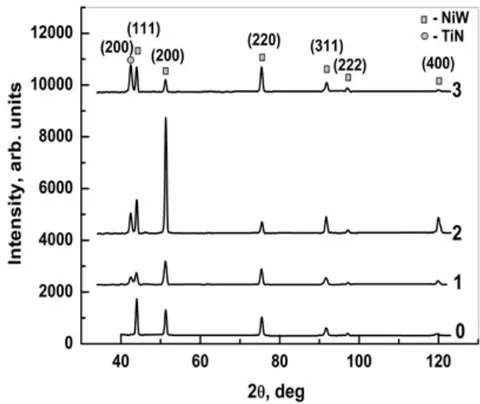
Fig. 5: XRD patterns of Ni
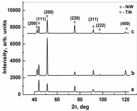
_{0.905} W _{0.095} alloy tapes with TiN coating ("Face") at p _{N} = 1.8 · 10 ^{-2} Torr in the range of 0 – 3 min (from the bottom up) As the deposition time \tau TiN increases up to 2 min, in other words as the coating thickness growths, the relative intensity of (h 0 0) type diffraction lines increases, while the intensities of reflections from the diagonal (h k 0) and other FCC lattice planes decreases. Such behavior of the evolution of diffraction pattern indicates qualitatively substantial intensification of degree of the cubic texture component in Ni_{0.905}W_{0.095} paramagnetic alloy tape. According to Fig. 6, that shows diffraction patterns of TiN/NiW systems obtained at different geometry of TiN deposition, mentioned above effect of texture enhancing is more apparent for the "face" coating geometry.
Fig. 5: XRD patterns of Ni 0.905 W 0.095 alloy tapes with TiN coating ("Face") at p N = 1.8 · 10 −2 Torr in the range of 0 – 3 min (from the bottom up) As the deposition time τ TiN increases up to 2 min, in other words as the coating thickness growths, the relative intensity of (h 0 0) type diffraction lines increases, while the intensities of reflections from the diagonal (h k 0) and other FCC lattice planes decreases. Such behavior of the evolution of diffraction pattern indicates qualitatively substantial intensification of degree of the cubic texture component in Ni0.905W0.095 paramagnetic alloy tape. According to Fig. 6, that shows diffraction patterns of TiN/NiW systems obtained at different geometry of TiN deposition, mentioned above effect of texture enhancing is more apparent for the "face" coating geometry.
Fig. 6: XRD patterns of Ni
_{0.905} W _{0.095} alloy tapes with TiN coating ("Face") at p _{N} = 1.8 · 10 ^{-2} Torr in the range of 0 – 3 min (from the bottom up). XRD patterns of Ni _{0.905} W _{0.095} alloy tapes with TiN coating obtained at optimized conditions at different coating geometry a) Original sample, b) Face, c) Shadow.
Fig. 6: XRD patterns of Ni 0.905 W 0.095 alloy tapes with TiN coating ("Face") at p N = 1.8 · 10 −2 Torr in the range of 0 – 3 min (from the bottom up). XRD patterns of Ni 0.905 W 0.095 alloy tapes with TiN coating obtained at optimized conditions at different coating geometry a) Original sample, b) Face, c) Shadow.

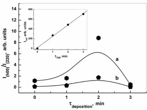
The Fig. 7 shows the dependency of texture parameter for Ni0.905W0.095 versus TiN coating deposition time.

Fig. 7: Dependency of
I_{(h00)} / I_{(220)} ratio from Ni_{0.905}W_{0.095} substrate on deposition time. Inset: Dependency I_{(200)}(\tau) for titanium nitride coating As can be seen it exhibits strong maximum at \tau_{TiN} = 2 min that corresponds to h_{TiN} \sim 1 \mu m. Process of cubic texture formation is also observed in the coating layer of TiN. This is proved by the presence of only (200)_{\mathrm{TiN}} diffraction line, which belong to cubic plane of the TiN lattice. The inset in the Fig 7 indicates that I_{(200)} from TiN monotonically increases in the whole range of \tau_{TiN}.
Fig. 7: Dependency of I(h00)/I(220) ratio from Ni0.905W0.095 substrate on deposition time. Inset: Dependency I(200)(τ) for titanium nitride coating As can be seen it exhibits strong maximum at τTiN=2 min that corresponds to hTiN∼1μm. Process of cubic texture formation is also observed in the coating layer of TiN. This is proved by the presence of only (200)TiN diffraction line, which belong to cubic plane of the TiN lattice. The inset in the Fig 7 indicates that I(200) from TiN monotonically increases in the whole range of τTiN.

In order to determine fine variations of texture in the TiN/Ni 0.905 W 0.095 system the algorithm of circular diagrams was used as a supplementation to the classical ways. This method is based on the construction and analysis of diagrams of the angular distribution of the intensity from crystallographic planes. In order to study the density of normals to (h k l) planes in various directions, a sample need to be rotated by angle ϕ about the normal to its surface.

As a criterion for the validity of the initial hypothesis regarding the realization of perfect cubic texture was chosen the known statistical method χ2. To calculate it n = 23 degrees of freedom were considered. Of course in the case of forming an ideal cubic texture, the value of "Chi - square" tends to be zero.

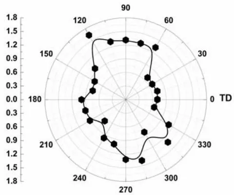
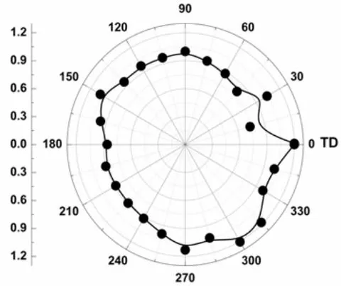
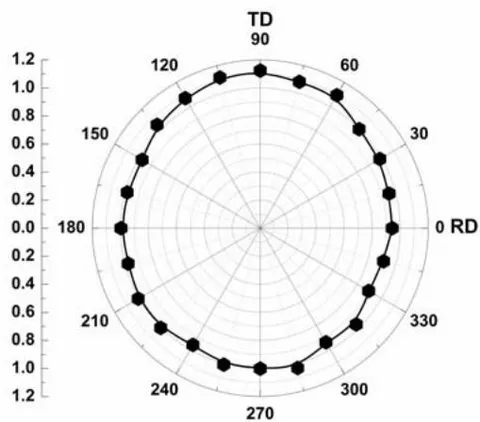
By way of illustration the Fig. 8 shows circular diagram from plane of type (h 0 0) for TiN coating at τ=2 min, where texture effects at which texture effects are most pronounced. The Fig. 9 shows circular diagrams from (2 0 0) plane related to Ni 0.905 W 0.095 subsystem before (Fig. 9a) and after coating (Fig. 9b) at optimized parameters:
hTiN=1μm,pN=1.8⋅10−2Torr.
Fig. 8: Circular diagram of (2 0 0) plane for TiN coating layer

It is worth to mention that for crystals belonging to cubic symmetry, the polar absorption tensor does not depend on the direction. Thus, any change in the intensity of the diffracted beam can be solely attributed to the processes of texture formation occurring in a two-layer system "substrate – coating".

One can see from the graphs above that the deposition of the TiN coating leads to the improvement of the cubic texture ( χtape=0.11→χcoated=0.07 ) in the metal component (Ni-W) of the two-layer system TiN / Ni0.905W0.095 as well as to formation of strong texture in coating layer ( χTiN=0.005 ).

IV. DISSCUSSOION

The subject of discussion in this paper is a set of observed effects related to the peculiarities of cubic texture formation in the thin-film system TiN/Ni 0.905 W 0.095 (see Fig. 3 – 9):

  1. Qualitative changes in the variation of the crystal lattice parameter dependencies of titanium nitride on the nitrogen pressure by varying the "geometry" of deposition during the experiment.

  2. The formation of rather strong cubic texture in metallic layer of the thin-layer system TiN/ Ni 0.905 W 0.095.

  3. The formation of quasi mono crystalline structure of TiN buffer layer in the system TiN/Ni 0.905 W 0.095.

Fig. 9: Circular diagram of (200) plane from a) original tape based on alloy Ni
_{0.905} W _{0.095} and b) subsystem
Fig. 9: Circular diagram of (200) plane from a) original tape based on alloy Ni 0.905 W 0.095 and b) subsystem

The identified differences in the dependences of the lattice parameters of titanium nitride may be caused by differences in the mechanisms and kinetics of the phase formation of TiN titanium nitride during deposition on different sides of the Ni-W tape. Dependence on the "front" side reflects the increase in the proportion of atoms with low atomic radius. On the "shadow" side the dependence reflects the mechanical reduction of titanium ion flux density due to deposition on the opposite side of the substrate. It is possible that the order of the reaction of the interaction of Ti and N ions may change.

The set of data presented in the figures 5 - 7 clearly indicates the processes of texture formation in substrate based on the paramagnetic alloy Ni0.905W0.095. under influence of TiN layer. This is clearly supported by the change of shape of intensity distribution from (200)NiW crystal plane as shown in the Fig.

The effect of an anomalous increase in the degree of cubic texture of the substrate, as well as the formation of a biaxial texture in the coating layer, is obviously associated with the process of reorientation of crystallites of both components of the TiN/Ni 0.905 W 0.095 system under the influence of interfacial stresses arising at the interface of materials with different values of the lattice parameters.

V. CONCLUSION

Ways to control the architecture of two-layer system TiN / Ni0.905W0.095 based on the change of nitrogen pressure during titanium evaporation, deposition time, and coating geometry were developed.

The conditions for creating two-layer "substrate – coating" compositions are optimized, which provide the possibility of obtaining strong cubic texture in the TiN coating layer deposited on the surface of the tape based on paramagnetic alloy Ni0.905W0.095.

The main result of the work is the experimental detection of the effect of correlated formation of a cubic texture in both components of the two-layer system TiN/Ni 0.905 W 0.095, which should provide a significant increase in critical current density of 2G HTS coated conductors.

References

34 Cites in Article
  1. 1. J Bednorz,K M�ller (1986). Possible highT c superconductivity in the Ba?La?Cu?O system. Zeitschrift f�r Physik B Condensed Matter, 64(2), 189-193.
  2. 2. M Paranthaman,C Park,X Cui,A Goyal,D Lee,P Martin,T Chirayil,D Verebelyi,D Norton,D Christen,D Kroeger (2000). YBa2Cu3O7-y−coated conductors with high engineering current density. Journal of Materials Research, 15(12), 2647-2652.
  3. 3. M Rupich,U Schoop,D Verebelyi,C Thieme,W Zhang,X Li,T Kodenkandath,N Nguyen,E Siegal,D Buczek,J Lynch,M Jowett,E Thompson,J-S Wang,J Scudiere,A Malozemoff,Q Li,S Annavarapu,S Cui,L Fritzemeier,B Aldrich,C Craven,F Niu,R Schwall,A Goyal,M Paranthaman (2003). YBCO coated conductors by an MOD/RABiTS/spl trade/ process. IEEE Transactions on Applied Superconductivity, 13(2), 2458-2461.
  4. 4. David Larbalestier,Alex Gurevich,D Feldmann,Anatoly Polyanskii (2001). High-Tc superconducting materials for electric power applications. Nature, 414(6861), 368-377.
  5. 5. W Hassenzahl (2001). Superconductivity, an enabling technology for 21st century power systems?. IEEE Transactions on Appiled Superconductivity, 11(1), 1447-1453.
  6. 6. M Wilson (1983). Superconducting Magnets. Superconducting Magnets
  7. 7. T Pyon,E Gregory (2001). Nb3Sn conductors for high energy physics and fusion applications. IEEE Trans. Appl. Supercond, 11, 3688-3691.
  8. 8. Yuh Shiohara,Takahiro Taneda,Masateru Yoshizumi (2012). Overview of Materials and Power Applications of Coated Conductors Project. Japanese Journal of Applied Physics, 51(1R), 010007.
  9. 9. A Malozemoff,S Annavarapu,L Fritzemeier,Q Li,V Prunier,M Rupich,C Thieme,W Zhang,A Goyal,M Paranthaman,D Lee (2000). Low-cost YBCO coated conductor technology. Superconductor Science and Technology, 13(5), 473-476.
  10. 10. Amit Goyal (2005). Epitaxial Superconductors on Rolling-Assisted-Biaxially-Textured-Substrates (RABiTS). Second-Generation HTS Conductors, 29-46.
  11. 11. E Specht,A Goyal,D Lee,F List,D Kroeger,M Paranthaman,R Williams,D Christen (1998). Cube-textured nickel substrates for high-temperature superconductors. Superconductor Science and Technology, 11(10), 945-949.
  12. 12. M Paranthaman,A Goyal,F List,E Specht,D Lee,P Martin,Qing He,D Christen,D Norton,J Budai,D Kroeger (1997). Growth of biaxially textured buffer layers on rolled-Ni substrates by electron beam evaporation. Physica C: Superconductivity, 275(3-4), 266-272.
  13. 13. M Wu,J Ashburn,C Torng,P Hor,R Meng,L Gao,Z Huang,Y Wang,C Chu (1987). Superconductivity at 93 K in a new mixed-phase Y-Ba-Cu-O compound system at ambient pressure. Physical Review Letters, 58(9), 908-910.
  14. 14. J Eickemeyer,D Selbmann,R Hühne,H Wendrock,J Hänisch,A Güth,L Schultz,B Holzapfel (2007). Elongated grains in textured substrate tapes and their effect on transport currents in superconductor layers. Applied Physics Letters, 90(1), 12510.
  15. 15. David Norton,Amit Goyal,John Budai,David Christen,Donald Kroeger,Eliot Specht,Qing He,Bernd Saffian,M Paranthaman,Charles Klabunde,Dominic Lee,Brian Sales,Fred List (1996). Epitaxial YBa 2 Cu 3 O 7 on Biaxially Textured Nickel (001): An Approach to Superconducting Tapes with High Critical Current Density. Science, 274(5288), 755-757.
  16. 16. Y Iijima,K Onabe,N Futaki,N Tanabe,N Sadakata,O Kohno,Y Ikeno (1905). Structural and transport properties of biaxially aligned YBa2Cu3O7−x films on polycrystalline Ni-based alloy with ion-beam-modified buffer layers. Journal of Applied Physics, 74(3), 1905-1911.
  17. 17. A Goyal,D Norton,J Budai,M Paranthaman,E Specht,D Kroeger,D Christen,Q He,B Saffian,F List,D Lee,P Martin,C Klabunde,E Hartfield,V Sikka (1996). High critical current density superconducting tapes by epitaxial deposition of YBa2Cu3Ox thick films on biaxially textured metals. Applied Physics Letters, 69(12), 1795-1797.
  18. 18. R Hühne,D Selbmann,J Eickemeyer,J Hänisch,B Holzapfel (2006). Preparation of buffer layer architectures for YBa2Cu3O7−xcoated conductors based on surface oxidized Ni tapes. Superconductor Science and Technology, 19(2), 169-174.
  19. 19. R Hühne,S Fähler,B Holzapfel (2004). Thin biaxially textured TiN films on amorphous substrates prepared by ion-beam assisted pulsed laser deposition. Appl. Phys. Lett, 85, 2744.
  20. 20. Ronald Gartner,Ruben Huhne,Jan Engelmann,Jens Hanisch,Rainer Kaltofen,Steffen Oswald,Ludwig Schultz,Bernhard Holzapfel (2010). High-$J_{\rm c}$ YBCO Coated Conductors Based on IBAD-TiN Using Stainless Steel Substrates. IEEE Transactions on Applied Superconductivity, 21(3), 2920-2923.
  21. 21. K Guth,R Huhne,V Matias,J Rowley,T Thersleff,L Schultz,B Holzapfel (2009). Preparation of Conductive Buffer Architectures Based on IBAD-TiN. IEEE Transactions on Applied Superconductivity, 19(3), 3447-3450.
  22. 22. J Thompson,A Goyal,D Christen,D Kroeger (2002). Ni–Cr textured substrates with reduced ferromagnetism for coated conductor applications. Physica C: Superconductivity, 370(3), 169-176.
  23. 23. U Gaitzsch,J Hänisch,R Hühne,C Rodig,J Freudenberger,B Holzapfel,L Schultz (2013). Highly alloyed Ni-W substrates for low AC loss applications. Superconductor Science and Technology, 26, 85024.
  24. 24. Subramanya Sarma,V Eickemeyer,J Schultz,L Holzapfel,B (2004). Recrystallisation texture and magnetisation behaviour of some FCC Ni-W alloys. Scr. Mater, 50, 953.
  25. 25. R Hühne,J Eickemeyer,V Sarma,A Güth,T Thersleff,J Freudenberger,O De Haas,M Weigand,J Durrell,L Schultz,B Holzapfel (2010). Application of textured highly alloyed Ni–W tapes for preparing coated conductor architectures. Superconductor Science and Technology, 23(3), 034015.
  26. 26. V Derevyanko,M Sungurov,T Sukhareva,V Finkel’,Yu. Shakhov (2018). Effect of the Composition and the Crystal Structure on the Electrophysical Properties of the Ni1–xWx System at Low Temperatures. Physics of the Solid State, 60(10), 1930-1934.
  27. 27. F Mohamed (1979). Creep behavior of solid solution alloys. Materials Science and Engineering, 38(1), 73-80.
  28. 28. V Finkel,A Bovda,V Derevyanko,S Leonov,M Sungurov,T Sukhareva,V Khoroshikh,Yu Shakhov (2012). Researches and developments on production of Ni-W alloy based substrates for second generation high-temperature superconductors. Functional Materials, 19(1), 109.
  29. 29. V Finkel (2013). Production of textured ribbons based on Ni–W paramagnetic alloys. Functional Materials, 20(1), 103-110.
  30. 30. I Aksenov,V Khoroshikh,N Lomino,V Ovcharenko,Y Zadneprovskiy (1999). Transformation of axial vacuum-arc plasma flows into radial streams and their use in coating deposition. IEEE Transactions on Plasma Science, 27(4), 1026-1029.
  31. 31. M Sungurov,V Derevyanko,S Leonov (2014). Substrates with a cubic texture based on paramagnetic Ni-W alloy ribbons with thin TiN coating for second-generation high-temperature superconductors. Tech. Phys. Lett, 40, 797-800.
  32. 32. H Friedman,L Birks (1946). Thickness Measurement of Thin Coatings by X -Ray Absorption. Review of Scientific Instruments, 17, 99.
  33. 33. I Tomov,S Vassilev (2007). Thickness Measurement of Thin Textured Films by a Novel X-Ray Diffraction Method Accounting for Secondary Extinction. Solid State Phenomena, 130, 43-46.
  34. 34. V Finkel,T Sukhareva,M Sungurov (2020). Detecting and determining the nature of an anomalous x-ray optical effect in two-Layer substrate–coating systems. Low Temperature Physics, 46(6), 594-598.

Funding

No external funding was declared for this work.

Conflict of Interest

The authors declare no conflict of interest.

Ethical Approval

No ethics committee approval was required for this article type.

Data Availability

Not applicable for this article.

How to Cite This Article

T. V. Sukhareva, M. S. Sunhurov, V. A. Finkel, Yu. N. Shahov. 2021. "Study of Two-layer System TiN / Ni 0.905 W 0.095 Adoptable for Creating Paramagnetic Substrates with Cubic Texture for 2G HTS Superconductors". Global Journal of Science Frontier Research - A: Physics & Space Science GJSFR-A Volume 21 (GJSFR Volume 21 Issue A2).

More Citation Formats

Download Citation

High-impact research on paramagnetic substrates for 2G HTS superconductors.
Journal Specifications

Crossref Journal DOI 10.17406/GJSFR

Print ISSN 0975-5896

e-ISSN 2249-4626

Keywords
Classification
GJSFR-A Classification FOR Code: 020399
Version of record

v1.2

Issue date
August 5, 2021

Language
English
Order Article Reprint
Experience in AR

Explore published articles in an immersive Augmented Reality environment. Our platform converts research papers into interactive 3D books, allowing readers to view and interact with content using AR and VR compatible devices.

Read in 3D

Your published article is automatically converted into a realistic 3D book. Flip through pages and read research papers in a more engaging and interactive format.

Article Matrices
Total Views: 772
Total Downloads: 62
All Trends

Request Access

Please fill out the form below to request access to this research paper. Your request will be reviewed by the editorial or author team.
X

This is the heading

Lorem ipsum dolor sit amet, consectetur adipiscing elit. Ut elit tellus, luctus nec ullamcorper mattis, pulvinar dapibus leo.

High-quality academic research articles on global topics and journals.

Study of Two-layer System TiN / Ni 0.905 W 0.095 Adoptable for Creating Paramagnetic Substrates with Cubic Texture for 2G HTS Superconductors

T. Sukhareva
T. Sukhareva
M. Sunhurov
M. Sunhurov
V. Finkel
V. Finkel
Yu. Shahov
Yu. Shahov